section epub:type=”chapter” role=”doc-chapter”> One of the key parameters in high temperature oxidation is the parabolic rate constant. This is true as long as protective oxidation determines the material behavior. Consequently, measurement of the weight change of the specimen is the key experimental technique in high temperature oxidation. Generally, there are two possibilities. The first is to take a number of specimens of the same type, expose them to the respective atmosphere in a closed furnace in which defined atmospheres can be established, and take the specimens out after different oxidation states. Before and after the tests, the specimens are weighed on a high‐resolution laboratory balance, and the weight change Δm provided by the surface area of the specimen, A, is plotted versus time. Therefore, before exposure, the surface area A of the specimens has to be determined accurately. If the results are plotted in a parabolic manner, that is, Δm/A is squared while t remains linear, the rate constant can be determined directly from the slope, as discussed in Chapter . A more elegant method is to use continuous thermogravimetry (Grabke and Meadowcroft 1995). In this case, a platinum or quartz string is attached to a laboratory balance that extends down into a furnace. At the lower end of the string, a coupon specimen is attached for which the surface area must be determined before the test. A movable furnace can also be installed that allows thermocyclic oxidation testing by periodically moving the furnace over and away from the specimen area. Ideally, the specimen should be in a quartz chamber or a chamber of another material that is highly corrosion resistant so that defined gas atmospheres can be used in the tests. The interior of the microbalance must be shielded against the aggressive gas atmospheres, usually by a counterflux of a nonreactive gas, such as argon. In a more sophisticated type of thermobalance, acoustic emission (AE) measurements can be made, for example, by acoustic emission thermography (AET) (see below; also Walter et al. 1993). This becomes possible if a waveguide wire is attached to the string hanging down from the balance, to which the specimen is attached. In particular, under thermocyclic conditions, AE measurements allow the determination of the critical conditions under which the oxide scales crack or spall (Schütze 1997). This type of scale damage is accompanied by mass loss due to spallation of the scale, and then this is directly reflected in the mass change measurements and can be correlated with AE results. In some situations, internal oxidation or corrosion may occur that cannot be detected directly by thermogravimetric measurements. Therefore, it is necessary to perform metallographic investigations as well. In particular, for continuous thermogravimetric testing, at the end of each test, a metallographic cross section should be prepared in order to check whether the mass change effects measured in the tests are caused by surface scales alone or whether the metal cross section has been significantly affected. Furthermore, if the kinetics of internal corrosion are to be determined, it is necessary to perform discontinuous tests where specimens are taken out of the test environment after different testing times and then investigated by metallographic techniques (Baboian 1995; Birks et al. 2006; Glaser et al. 1994; Wouters et al. 1997). Standard high temperature corrosion investigations also usually include an analysis of the corrosion products formed in the tests or under practical conditions because this allows conclusions as to which are the detrimental species in the environment and whether protective scales had formed. In most cases, this is done either in the scanning electron microscope (SEM) by using energy‐dispersive X‐ray analysis (EDX) or with metallographic cross sections in the electron probe microanalyzer (wavelength‐dispersive X‐ray analysis, WDX). Another tool may be glancing angle X‐ray diffraction (GAXRD) technique, which allows analysis of the composition of thin layers. Common experimental investigation techniques used to assess corrosion morphology, identify corrosion products, and evaluate mechanical properties are the following (Birks et al. 2006; Marcus and Mansfeld 2006; Rahmel 1982; Sequeira et al. 2008; Taniguchi et al. 2006): Optical microscopy Scanning electron microscopy (SEM) Electron probe microanalysis (EPMA) Transmission electron microscopy (TEM) X‐ray diffraction (XRD) Energy‐dispersive X‐ray analysis (EDX) Secondary ion mass spectroscopy (SIMS) X‐ray photoelectron spectroscopy (XPS) Auger electron spectroscopy (AES) Laser Raman spectroscopy (LRS) Creep rupture Postexposure ductility Modulus of rupture (MOR). In general, creep rupture, hardness, and MOR have been used equally to assess the mechanical properties of corroded test pieces. When the material is difficult to grip (as is a ceramic), its strength can be measured in bending. The MOR is the maximum surface stress in a bent beam at the instant of failure (International System [IS] units, megapascals; centimeter–gram–second units, 107 dyn cm−2). One might expect this to be exactly the same as the strength measured in tension, but it is always larger (by a factor of about 1.3) because the volume subjected to the maximum stress is small and the probability of a large flaw lying in the highly stressed region is also small. (In tension all flaws see the maximum stress.) The MOR strictly applies only to brittle materials. For ductile materials, the MOR entry in the database is the ultimate strength. The technical domains in which high temperature corrosion is of importance include thermal machines, chemical industry, incineration of domestic or industrial waste, electric heating devices, and nuclear engineering, and apart from purely environmental aspects, high temperature corrosion also constitutes a stage of some industrial processes of high financial or human cost (e.g. materials preparation with controlled properties, thermochemical surface treatment processes, etc.). Therefore, besides the oxidation problems discussed above, high temperature corrosion also involves other gaseous atmospheres (N2, S2, Cl2, etc.), molten liquids (salts, metals, etc.), and more complex environments. Therefore, it is clear that to attain the expected performances of the systems and devices subjected to high temperature corrosion, as well as to characterize the corrosion scales and understand the corrosion mechanisms, it is necessary to use many experimental techniques. These include spectroscopic, electrochemical, and many other complex techniques. Spectroscopic techniques used for analysis of corrosion problems and characterization of thin and thick layers of corrosion scales are of considerable importance, but electrochemical techniques and other techniques using indirect measurements for the study of solid‐to‐solid, solid‐to‐liquid, and solid‐to‐gas properties are now becoming of great interest. In the next section, brief considerations are included on the basic testing equipment and monitoring, at laboratory scale, as well as on optical microscopy and thermogravimetry. Then, a very brief summary of the main spectroscopic techniques in current use, their main limitations, and scope for development is provided. In fact, spectroscopic techniques used for chemical analysis of oxidation problems and characterization of thin layers of corrosion scales are more and more of considerable importance, thus deserving an entire section for their general discussion. In the following sections, numerous former and actual experimental techniques are considered, being possible to obtain more detailed methodology or results of specific techniques. In these sections, nondestructive inspection (NDI) techniques are also included. The effects of temperature on mass transport and kinetics phenomena of corrosion nature along with its use in a number of technological industries of particular interest, such as nuclear, fossil‐fueled, geothermal, high temperature fuel cells and high‐energy batteries, and so on, require the knowledge of detailed mechanistic studies involving high temperature aqueous and solid‐state electrochemistry. Thus, a number of electrochemical techniques and procedures are discussed in the last section of this chapter. The reaction vessels for studying high temperature corrosion may be horizontal or vertical tubes, depending on the type of measurement required. Pyrex glass can be used up to 450 °C only and must be changed to vitreous silica (often improperly called “quartz”) that can then be used up to 1050 °C. These glassy materials have the advantage of being transparent to light and of being joined and readily molded to shape by flame processing. For higher temperatures, ceramic materials such as mullite or alumina should be employed. Metallic reaction vessels are seldom used since they themselves may react with the oxidizing gas. For studies of corrosion by fluorine, F2, or its compounds such as HF, SOF2, or SO2F2, it should be noted that silica glasses are not stable, and, similarly, for halogen–carbon reactions where alumina is chlorinated, nickel‐based alloys are used. It will also be necessary to use metallic vessels (termed autoclaves) when high pressure reactions are studied. Tubular electric furnaces are of common use in air up to 1250 °C with metal wire heating elements (NiCr, FeCrAl, NiCrAl), but, for higher temperatures, these elements have to be protected against oxidation. Heating elements made of SiC or MoSi2 are self‐protecting through the formation of a silica layer, and their use extends the temperature range of air furnaces to 1500 °C. Tungsten or molybdenum resistance furnaces can be used up to 2500 °C, provided that they are kept under vacuum to prevent oxide volatilization. Reliable measurement of test temperature is of great importance because of the strong dependence of the reaction kinetics on temperature. Several types of thermocouples are available, depending on the temperature range being used: The higher the maximum temperature for these couples, the lower their sensitivity. Locating the thermocouple inside the reaction is obviously the best option for accurate temperature measurement, but the thermocouple in relation to the specimen within the furnace is also of major importance. A location inside the reactor tube would obviously be better. For particularly corrosive environments, it is sometimes useful to use stainless steel or Inconel sheeting, particularly for the K‐type thermocouples. When the thermocouple tip has to be placed inside the reaction vessel, careful calibration measurements have to be performed to map the longitudinal and radial temperature gradients within the furnace. In all cases, effective draft proofing has to be placed at both ends of the furnace, between the reactor and furnace tubes, to avoid air convection currents that would disturb the temperature distribution within the vessel. The use of such insulation is particularly recommended for vertical furnaces. Static or dynamic atmospheres may be used during oxidation testing. For the case of static atmospheres, the oxidant, usually a gas, is introduced into the reaction chamber after it has been evacuated, and the reaction vessel is then subsequently closed. Such atmospheres are characterized by the total pressure and the molar fraction (partial pressures, in the case of a gas) of each constituent. For the case of dynamic atmospheres, the oxidant continuously circulates in the open reaction chamber. The flow rate is then an additional experimental variable, and it is necessary to know this as part of the complete characterization of the oxidation test. Static atmospheres should be used only when the reactive oxidizing species, assumed gaseous for illustration, are in overwhelmingly large concentrations so that the products of reaction do not have any significant effect on the original concentration. In all other cases, only dynamic atmospheres can ensure constant partial pressures of the reacting constituents and control over the buildup of reaction products. Gas flow rates in the range of 0.1–10 mm s−1 are commonly used, but simple mass balance calculations can ensure that the concentration of oxidant is in large excess compared with the amount lost during the reaction. This condition has to be fulfilled to avoid affecting the kinetics of reaction through a limitation on the supply of oxidant. Such a limitation may occur, for example, when very small amounts of highly reactive gases (HCl, SO2, etc.) are diluted in an inert carrier gas. Experiments conducted at different flow rates can be usefully used to establish whether kinetic limitations apply for particular test conditions. To monitor the extent of the corrosion reaction, a few common approaches are described below. Laboratory testing equipment and experimental monitoring of the corrosion extent other than oxidation processes are also briefly described in the context of the techniques analyzed below. Optical microscopy is a very common technique used for the corrosion morphology assessment, and it is outlined here for studying carbons and other lamellar structures. Specimens are prepared by mounting the sample in a resin block and polishing the surface to optical flatness using alumina or diamond paste (if the specimen is massive enough, it can be polished without mounting). The polished surface is examined using reflected light microscopy usually with polarized light. To observe interference colors, due to the orientation of the graphitic lamellae at the surface, parallel polars are used with a half‐wave retarder plate between the specimen and the analyzer. The general arrangement is shown in Figure 17.1, together with diagrams illustrating the generation of the interference colors. Figure 17.1 Polarized light optical microscopy and interference colors. The appearance of a surface is called its optical texture. Figures 17.2–17.4 illustrate the type of textures observed. The size and shape of the isochromatic areas can be estimated. Dimensions vary from the limit of resolution ∼0.5 µm to hundreds of micrometers. The nomenclature used to describe the features has been developed over many years, and discussions are still underway to establish a more standard system. Table 17.1 gives definitions of the classes of optical anisotropy together with a definition of optical texture index (OTI), factor that is useful for characterizing a carbon material. Figure 17.2 Optical micrograph of coke surface – fine‐grained mosaic, OTI = 1. Figure 17.3 Optical micrograph of coke surface – medium and coarse mosaic, OTI = 3. Figure 17.4 Optical micrograph of coke surface – coarse flow, OTI = 30. Table 17.1 Description of optical anisotropy and OTI By point counting the individual components of the microscope image and multiplying the fraction of points encountered for each component by the corresponding OTI factor and summing the values, the optical texture index for the sample can be obtained. This number gives a measure of the overall anisotropy of the carbon. It must be stressed that this is only a comparative technique and that material characterized as isotropic may only be so at the level of resolution. This becomes obvious when a surface is examined with a higher‐grade objective (not just higher power), allowing more anisotropy to be observed (distinguished). Other uses of optical microscopy in the study of carbon materials are mainly concerned with coal petrography, a discipline based on the measurement of reflectance from the coal surface and dealing with coal materials in terms of macerals. These forms are identifiable as deriving from the original plant material via the coalification process. A related area is the study of char forms derived from the pyrolysis of coal. The most widely used method to follow the kinetics of high temperature oxidation and corrosion is to measure the mass change (amount of metal consumed, amount of gas consumed, amount of scale produced) with temperature: thermogravimetry. The simplest method of mass change monitoring is to use a continuous automatic recording balance. The apparatus suitable for this is shown diagrammatically in Figure 17.5, which is self‐explanatory. Figure 17.5 Typical experimental arrangement for measuring oxidation kinetics with an automatic recording balance (Birks et al. 2006). To increase the accuracy of these balances toward the microgram range, the physical interactions of the sample with the gas must be taken into account and combated. Three of these interactions are of importance. Thermogravimetric kinetic measurement will be perturbed, and errors introduced in all cases where buoyancy varies with time. To illustrate this, consider a solid of volume V immersed at temperature T in a perfect gas mixture of mean molar mass M at a pressure P. The effect of buoyancy can then be described by where g is the acceleration due to gravity and α the ratio T°/P°V° of the temperature, pressure, and molar volume of gases under normal conditions. This relation first shows that buoyancy depends on temperature so that temperature variations during the experiment lead to apparent mass changes, but these are easy to calculate. As example, consider a typical rectangular sample with dimensions 20 × 10 × 2 mm3 placed in oxygen. Heating this sample from room temperature to 1000 °C will lead to an apparent increase in mass of approximately 0.5 mg. It can be ascertained that, to achieve maximum balance sensitivity under nominally isothermal measurements, care must be taken to ensure a high standard of temperature control of the furnace. For example, with temperature variations of ±3 °C near 300 °C, the apparent mass variations are of the order of ±2 µg; at higher temperatures, the error in the determination of mass is less, e.g. ±0.3 µg at 1000 °C, because of the lower gas density. Buoyancy force variations with the increase of sample volume during oxidation can also be calculated but are generally negligible compared with the accuracy of the thermobalances. Convection currents result from the effect of gravity on temperature‐induced differences in the specific mass of gas at different locations within the reaction vessel. They become noticeable for pressures greater than 100–200 mbar and are manifested by convection loops that can perturb the thermogravimetric measurements. In open static reaction vessels, the convection loops curl outside the reaction vessel, and the well‐known chimney effect is observed (Figure 17.6a). Such a configuration has to be avoided, or one end of the reaction vessel has to be plugged. Figure 17.6 Convection currents in reaction vessels. (a) Vertical open vessel. (b) Closed static vessel. In closed static reaction vessels, convection may occur due to radial temperature gradients, as shown schematically in Figure 17.6b where the sample is envisaged to have a temperature slightly lower than that of the vessel wall. The convection loops in this case lead to an apparent mass increase. Near the top of the furnace, where strong radial and longitudinal gradients are present, convection phenomena are present. Such a region (20 cm above the furnace) is subject to turbulence that may be minimized by the use of thin suspension wires having no geometrical irregularities such as asperities or suspension hooks. A semiquantitative assessment of the importance of these natural thermal gravity convection currents can be obtained through the use of the Rayleigh number, Ra. This dimensionless number is defined as where g is the acceleration due to gravity, β the coefficient of thermal expansion of the gas (for a perfect gas: β = 1/T), Cp the thermal capacity of the gas at constant pressure, ρ the density of the gas, b the length of the non‐isothermal zone, ΔT the temperature difference, η the dynamic viscosity of the gas, and K the thermal conductivity of the gas. For low values of the Rayleigh number (Ra < 40 000), natural thermal gravity convection may be neglected. For higher values, convection loops may perturb thermogravimetric measurements, sometimes creating very strong movements of the sample suspension system and leading to a drastic decrease in accuracy. In dynamic reaction vessels, the imposed gas flow leads to forced convection whose effects are generally greater than those due to natural convection. The flow behavior within the vessel can then be described by the Reynolds number (Re). This dimensionless number is defined as where ρ is the density of the gas, u the linear velocity of the gas, L the characteristic length of the system, and η the dynamic viscosity of the gas, calculated using the following equation: where k is the Boltzmann’s constant, m the mass of one gas molecule, T the absolute temperature of the reaction vessel, and σ the mean collisional cross section of a molecule (σ = 4πr2, where r is the molecule radius). This approach, though necessarily simple, provides insights into the factors that affect the accuracy of the experimental values obtained in thermogravimetric tests. It should be noted that the values given for the Rayleigh and Reynolds numbers have to be considered as an order‐of‐magnitude guide only. For example, a gas flow with a Reynolds number of 2000 may be turbulent in a tube of high internal roughness but perfectly laminar in a smooth silica tube. In contrast to convection forces, which are active at moderate and high gas pressures, thermomolecular fluxes appear at low pressures in the domain where the gas may be considered as a Knudsen gas. The term Knudsen gas describes a situation where molecules do not collide with each other but only with the vessel wall. Such behavior occurs for values greater than 1 of the dimensionless Knudsen number (Kn): where λ is the mean free path of molecules and d is a characteristic distance, e.g. the tube radius for a cylindrical reaction vessel. In this Knudsen domain, gas pressure relates to temperature according to Consider a cylindrical sample immersed in a Knudsen gas and submitted to a temperature difference T2 − T1 applied across a horizontal plane whose trace is XY in Figure 17.7. This sample is then submitted to two resulting Knudsen forces: Figure 17.7 Normal and tangential forces acting on a vertical cylindrical sample submitted to a temperature gradient in a Knudsen gas. The resulting force Fn arises from the difference in the pressure forces on the two circular bases of the cylinder (Figure 17.7a): The resulting tangential force is due to the difference in the momentum of the molecules hitting the vertical surface of the sample and arriving from the upper (hot) or the lower (cold) part of the reaction vessel (Figure 17.7b). Such a force was forecasted by Maxwell (1973). It can be expressed by In the intermediate domain, defined by a Knudsen number between 1 and 10−5, normal and tangential forces are the result of a gas flux generated according to the exchange of momentum between molecules. The calculation of these forces is complex, but it can be shown that they increase with pressure and pass through a maximum before they decrease. This decrease results from the modification of gas properties and the appearance of a regime where the pressure in a closed isothermal vessel has a unique value. Table 17.2 describes the different gas flow phenomena that may perturb thermogravimetric measurements and identifies the domains where they are active. Table 17.2 Gas flow regimes where perturbation of thermogravimetric measurements may occur Table 17.3 Methods of material characterization by excitation and emission In order to limit all the perturbations described above, a symmetrical furnace setup is particularly efficient. In order to optimize performance, both furnaces are operated as nearly as possible at the same temperature and with the same temperature gradients. Setaram, for example, supplies accurate thermobalances of this type of symmetrical furnaces. Chemical analysis by spectroscopy has made rapid advances in high temperature studies and almost always includes equipment for high‐resolution microscopy. Several books and monographs are available, including most of the old and newly developed techniques (Kofstad 1988; Marcus and Mansfeld 2006). Glow discharge mass spectroscopy (GDMS) is fast, sensitive, accurate, simple, and reliable and can be used for surface analysis if the specimen can be attached to a vacuum cell (Bernéron and Charbonnier 1982). The resolving power in‐depth profiling is similar to AES and SIMS. A 1 kV glow discharge causes ion bombardment and surface erosion that is fed (optically) to a multichannel spectrometer for elemental analyses. Other long and complex methods of surface analysis, such as AES, SIMS, XPS, ISS (ion scattering spectroscopy), RBS, NRA, IIXA (ion‐induced X‐ray emission), and ESCA (electron spectroscopy for chemical analysis), are difficult for field use. Several authors have reviewed these methods. Tables 17.3–17.6 compare the techniques, and Figure 17.8 shows the relative sizes of areas analyzed using these techniques. Table 17.4 Summary of various characteristics of the analytical techniques Table 17.5 Outline of some important techniques to study metallic surfaces Table 17.6 Types of samples and techniques nearly appropriate for their analysis Figure 17.8 Schematic illustrating relative sizes of areas scanned by spectrometric analytical techniques. Commonly used methods are optical and SEM for surface studies. TEM of interfaces has been explored. Selected area diffraction patterns (SADPs) show the orientation between different grains. In a ceramic coating, the interface between different phases can be coherent, semi‐coherent, or incoherent. Coherent phases are usually strained and can be studied by TEM contrast analysis. Other aspects of analytical electron microscopy analysis are discussed (Hansmann and Mosle 1982; Thoma 1986). TEM resolution is better than 1 nm, and selected volumes of 3 nm diameter can be chemically analyzed. Methods of preparing thin TEM transparent foils are described (Doychak et al. 1989; Lang 1983). Photoemission with synchrotron radiation can probe surfaces of an atomic scale (Ashworth et al. 1980; Pask and Evans 1980), but this method requires expensive equipment. Complex impedance measurements can separate surface and bulk effects, but problems of interpretation still need to be resolved (Marcus and Mansfeld 2006). X‐ray and gamma radiographs, as used in weld inspection, can be used to inspect coating for defects. The method has been discussed by Helmshaw (1982). Inclusions, cracks, porosity, and sometimes lack of fusion can be detected. Surface compositions of ion‐implanted metals have been studied by RBS (Brewis 1982; Marcus and Mansfeld 2006). In this nondestructive way, a microanalysis of the near‐surface region is obtained. Interpretation is relatively easy. Assessment of radiation damage in ion‐implanted metals by electron channeling is described using SEM (Ashworth et al. 1980) for the characterization of surface films (Marcus and Mansfeld 2006). AES and XPS analyze the top of the surface only, and erosion by ion bombardment or mechanical tapering is needed to analyze deeper regions. AES detects 0.1% of an impurity monolayer in a surface. Auger electrons are produced by bombarding the surface with low‐energy (1–10 keV) electrons. In XPS the surface is exposed to a soft X‐ray source, and characteristic photoelectrons are omitted. Both AES and XPS electrons can escape from only 1 nm depth from the surface, and so these are surface analytical methods (Brewis 1982; Marcus and Mansfeld 2006). It is most important to avoid contamination during preparation for surface analysis; semiquantitative in situ analysis by AES has been reported (Bosseboeuf and Bouchier 1985). Nitrides and other compound refractory coatings are frequently analyzed by AES and RBS methods. Depth and crater edge profiling have been carried out for direct‐current (DC) magnetron sputtered and activated reactive evaporation (ARE) samples of (Ti, Al)N, TiN, and TiC coatings (John et al. 1987; Kaufherr et al. 1987). Round‐robin tests of characterization by including a range of analyses such as XPS, EPMA, XRS, AES, APMA, and XRD are not uncommon. Among these, XRD was felt to be unreliable (Perry et al. 1987). Ion spectroscopy is a useful technique for surface analysis (Marcus and Mansfeld 2006). ISS uses low‐energy backscattered ions (Czanderna 1975) and has a high sensitivity. SIMS has the possibility of sputter removal of layers, allowing depth profiling (Brewis 1982). It can act as a stand‐alone system to solve surface analysis. Three‐dimensional (3D) SIMS of surface‐modified materials and examination of ion implantation is reported (Fleming et al. 1987). Lattice vacancy estimation by positron annihilation is another approach (Brunner and Perry 1987). TEM and SEM are valuable techniques, and replication methods using, for example, acetate replicas can nondestructively reveal surface features of specimens too thick for TEM (Brewis 1982; Grabke and Meadowcroft 1995). ARE coatings of V–Ti in C2H2 give wear‐resistant (V, Ti)C coatings. The hardness is related to grain size, stoichiometry, free graphite, and cavity networks. SEM and XRD analysis could not be used to explain the large hardness variations obtained by varying temperature and gas pressure, but TEM revealed microstructural changes (Grabke and Meadowcroft 1995; Lang 1983; Marcus and Mansfeld 2006). Beta backscatter and X‐ray fluorescence have low sensitivity (0.5 cm2 min−1 and 1 cm2 h−1, respectively). Thickness and uniformity of silica coatings on steel have been determined by X‐ray fluorescence measurements of Si concentrations along the surface (Bennett 1984; Lang 1983). Round‐robin tests for microstructure and microchemical characterization of hard coatings have included XPS, UPS (UV photoelectron spectroscopy), AES, EELS (electron energy loss spectroscopy), EDX, WDX (wave‐dispersive X‐ray analysis), RBS, SIMS, TEM, STEM (scanning transmission electron microscope), and XTEM (X‐ray transmission electron microscopy) (Bennett 1984; Bennett and Tuson 1989). Field emission STEM has been applied for profiling Y across a spinel–spinel grain boundary (Bennett 1984; Bose 2007; Grabke and Meadowcroft 1995; Sundgren et al. 1986). In summary, when studying oxidation behavior at high temperatures, the foremost requirement is to monitor the extent and kinetics of attack. To obtain a complete mechanism understanding, such data have to be augmented by precise details of all the processes involved, starting with the chemical reaction sequence, leading to the formation of gaseous products and solid products at the reacting surface. The development and failure of protective surface scales crucially govern the resistance of most materials in aggressive environments at elevated temperatures. Knowledge is also essential on the changes throughout the exposures of the scale chemical composition, physical structure (including topography), stress state, and mechanical properties as well as on the scale failure sequence (e.g. by cracking and spallation). All these processes involved in high temperature oxidation are dynamic. Therefore, to obtain unambiguous information, the main experimental approach in research should be based on in situ methods. These can be defined as being techniques that either measure or observe directly high temperature oxidation processes, as they happen in real time. Although numerous in situ methods have been developed to date, with several notable exceptions, the most important being controlled atmosphere thermogravimetry, the deployment of these techniques has been often limited. This may be attributed largely to experimental difficulty and also to the lack of suitable equipment. Current understanding of the chemical and physical characteristics, stress state, and mechanical properties of oxidation scales largely derives from postoxidation investigations. In fact, certain detailed aspects, for example, variations in mechanical properties and microstructure through scales, can be revealed only by postoxidation studies. The two main experimental approaches, in situ oxidation and postoxidation, are not mutually exclusive, as they complement and augment each other. Nevertheless, at the current state of mechanistic knowledge of high temperature oxidation, further understanding of many critical facets (e.g. the breakdown of protective scales) will be revealed only by real‐time experimentation. These requirements taken in conjunction with recent advances in both commercial and experimental equipment design/capabilities and in data storage/processing make it imperative that all investigators in this field be fully aware of the available in situ experimental test methods. The purpose of this section is to provide a very brief summary of some major techniques in current use, their main limitations, and scope for development. Information on the detailed methodology of any technique or the complete results of any specific study using any such technique should be obtainable from the following sections and/or the references given to published papers. Diffraction techniques are the most important to the analysis of crystalline solids – both phase and structural information. The techniques of greatest interest in this area include XRD, low‐energy electron diffraction (LEED), reflection high‐energy electron diffraction (RHEED), and neutron scattering. XRD is included even though it is not a surface‐specific technique since it is by far the most common of the diffraction‐based techniques used, i.e. this is the standard method for solving crystal structures for both single‐crystal samples and powdered crystalline samples. Surface specificity is lost in XRD due to the geometry used and the fact that photons have long path lengths within solids for both elastic and inelastic collisions. The remainder are surface‐specific techniques. The average bulk structure of many materials can be readily revealed using XRD. The technique provides a measure of the amount of ordered material present and can be used to give an indication of the size of the crystallites that make up the ordered structure. The samples are usually prepared either as powders in capillaries or spread on a flat sample holder. The XRD pattern is recorded either on film or with a diffractometer. Figure 17.9 shows the arrangement of a powder diffractometer. Figure 17.9 X‐ray diffraction. The resulting pattern is the amount of scattering over a range of scattering angles, θ, and can be analyzed in terms of diffraction peaks, their positions, and their widths. For the most accurate work, a standard (usually a crystalline salt) is added to the powder to provide internal calibration of the peak positions and widths, thereby allowing any instrumental factors to be taken into account. Although the main scattering derives from the ordered material present, some indication of the amount of disorder can be obtained by the background scatter. Similarly, the broadening of the diffraction peaks allows an estimation of the mean particle size to be made. Line broadening arises from both the strain or defects in the lattice and the finite crystal size. Assuming that the defects in the lattice reduce the extent of order, an effective crystallite size, t, can be estimated from the amount of broadening, β, using the Scherrer equation where λ is the wavelength, θ is the scattering angle, and the value of κ (∼1) depends upon the shape of the crystallite, e.g. κ has the values of 0.9 for Lc and 1.84 for La. β is the amount of broadening due to the sample, and the observed broadening, B, usually needs to be corrected for the instrumental broadening, b, using relationships such as The measuring of line broadening is illustrated in Figure 17.10. Figure 17.10 X‐ray diffraction line broadening. The parameters usually quoted from XRD experiments are These give some indication of the degree of crystallization of the material. One specialized area of diffraction is that of fiber diffraction. Both normal and small‐angle scattering patterns are used for this investigation. Materials with large surface area can also be successfully investigated by a combination of small (low) and normal (high) angle scattering. Small‐angle scattering has also been used to give some indication of pore structure. Scattering of electrons from solid surfaces is one of the paradigms of quantum physics. The pioneering experiments of Davisson and Germer, in 1928, confirmed the Broglie’s concept of the wave nature of particles (de Broglie 1925), a concept at the very heart of quantum mechanics (wave–particle dualism). Already in these early works, they recognized the potential of LEED as a tool for the determination of surface structures and applied it to gas adsorbate layers on Ni(111) (Davisson and Germer 1928a,b). This success was only possible due to two important properties of LEED: surface sensitivity and interference. In fact, an alternation of the electron beam intensity with sample thickness was observed by Davisson and Germer (1928a,b). Electrons in an LEED experiment have a typical kinetic energy in the range of 20–500 eV. Experiments with energies below this range are called very low‐energy electron diffraction (VLEED), and those with higher energies medium‐energy electron diffraction (MEED). At even higher energies, one uses grazing electron incidence and emission to obtain surface sensitivity, that is, RHEED. Due to the interaction of the incoming electron with the electrons in the sample, the former penetrates into the solid only a few angstroms. Typical penetration lengths taken from the “universal curve” (Figure 17.11) range from 5 to 10 Å (Rundgren 1999). Therefore, LEED spectra usually carry less information about the geometrical structure of the volume of the solid, i.e. the bulk, than of the solid’s surface region. Figure 17.11 Compilation for elements of the inelastic mean free path λm (dots) in monolayers as a function of energy above the Fermi level. This “universal curve” is almost independent of the solid, for example, surface orientation of elemental composition. The solid line serves as a guide to the eye (Seah and Dench 1979). Concerning interference, de Broglie showed that a particle with momentum p can be associated with a wave with wavelength 2π/p (p = |p|). For example, an electron in vacuum can be described by a plane wave: with wavenumber k = 2π/λ and energy E = ω = k2/2. de Broglie’s picture of electrons as waves and the interpretation of Davisson–Germer LEED experiments lead to the question: Are electrons waves? (Davisson 1928). Comparison was made to X‐ray scattering in view of the determination of structural information, and Davisson came to the conclusion that if X‐rays are waves, then electrons are, too. However, he/she admitted that the picture of electrons as particles is better suited for the explanation of the Compton effect or the photoelectric effect. The schematic setup of a LEED experiment is shown in Figure 17.12. A monoenergetic beam of electrons with kinetic energy E impinges on the sample. The reflected electron beams are detected and analyzed with respect to their direction and energy. Usually, one detects only elastically reflected electrons (for which the energy is conserved) and uses incidence normal to the surface. Therefore, a set of LEED spectra – or I(E) curves – represents the current I of each reflected beam versus the initial energy E. Note that the reflected intensities are roughly as large as 1/1000 of the incoming intensity. Figure 17.12 Scheme of the LEED setup. An incoming beam of electrons e− is elastically scattered by the solid. The latter is considered as a compound of the substrate (gray circles) and a thin film (black circles). A reflected electron beam is detected. The dashed–dotted arrow represents the normal surface. In the wave picture of electrons, the LEED experiment can be regarded as follows. An incoming plane wave, the incident beam, is scattered at each site, and the outgoing plane waves, the outgoing beams, are measured. Both amplitude and phases of each outgoing wave are determined by the scattering properties and the position of each scatterer. For example, a change in the position of a scatterer will change the wave pattern in the solid and, therefore, will affect both amplitudes and phases of the outgoing waves. Because the LEED current of a beam is given by the wave amplitude, it carries information on both positions and scattering properties of the sites. This mechanism can be used, for instance, to obtain images of the geometrical structure in configuration space by LEED holography (Heinz et al. 2000). Although LEED is sensitive to the outermost region of the sample, it is capable of detecting fingerprints of the electronic states of the film–substrate system. As mentioned previously, the LEED intensities depend on the electronic structure of the sample above the vacuum level and, therefore, contain information of the electronic structure of the entire film. In particular, quantized states that are confined to the film have a pronounced effect on the LEED spectra. It took considerable time to develop theories that include multiple scattering of the LEED electron (Kambe 1967), which obviously is necessary for a proper description of LEED spectra. Textbooks that are introduced to the field and present computer codes for the calculation of I(E) spectra were written by Pendry (1974) as well as van Hove et al. (1986). Van Hove and Tong also provide review articles (1979). Additional information can be obtained if one uses a spin‐polarized beam of incoming electrons, that is, spin‐polarized low‐energy electron diffraction (SPLEED), and uses a spin‐sensitive detector, for example, a Mott detector or a SPLEED detector. Interestingly, the latter exploits the LEED mechanism itself for a spin resolution in the experiment. Pioneering works were carried out by Feder (1985) and by Kirschner and Feder (1979) on the experimental side. The short history of RHEED study of oxides is relatively recent, and good general introductions to this matter date from Lagally (1985) and Lagally and Savage (1993); there one can find a clear explanation of the electron diffraction, reciprocal‐space representation, reflection from imperfect surfaces, and so on. RHEED patterns result from and contain detailed information on the crystalline properties of surfaces. In the field of oxide thin films, RHEED analysis is currently used mainly for qualitative information, simply to watch diffraction problems and to note their evolution in time. Even this can be quite useful and can reveal atomic scale information on how a sample is growing with reference to phenomenology developed by experience. As discussed below, it is possible to distinguish a flat two‐dimensional (2D) surface from one having (usually unwanted) 3D nanoparticles. For the time being, we consider the former case. At least in principle, the diagnostic value of RHEED monitoring could be substantially increased if it were supplemented by a quantitative analysis of the entire RHEED pattern. Ultimately, one could envision a numerical routine that solves the inverse problem in real time, that is, computes the real‐space atomic arrangement on the surface that corresponds to a given RHEED image. In Figure 17.13, a schematic of a typical calculation and of an experimental RHEED setup is shown. The electron beam (E) impinges onto the film surface (F) at a nearly grazing angle (θ) and is reflected (E′) onto the screen (S). Figure 17.13 The model used in this chapter to calculate RHEED patterns. The electron beam (E) impinges onto the film (F) at a nearly grazing angle (0). The reflected beam (E′) forms a diffraction pattern on the screen S. The electron beam is coherent over several thousand angstroms and is nearly monoenergetic; in our case, the electron energy is typically ≈8.5–10.0 keV. The film surface is approximated as a perfect but finite rectangular N × M array of atoms with the lattice periods a and b, respectively. Since typically a ≈ b ≈ 4 Å > λe ≈ 0.15 Å, the electrons are strongly diffracted, and one expects to see multiple interference maxima on the screen. In this case, the refinement procedure provides an estimate of the size of in‐plane crystallographic coherence, that is, an estimate of the numbers N and M. To calculate the diffraction pattern, the scattering contributions from all of the atoms are summed. The resulting intensity distribution on the screen is given by where and where E and m are the electron energy and mass and r = (ia)ex + (ja)ez, Ra, Xaex + Yaey + Zaez and R = Xex + Yey + Zez are the positions of the (i, j)th atom in the plaquette, the electron source, and the screen pixel, respectively. When the atoms are not all identical, their contributions are weighted by the respective form factors, Sij (not shown in Eq. 17.13). As the first step to aid the reader’s intuition, in Figure 17.13 we show the calculated RHEED patterns for three ideal but finite atomic lattices, 10 × 10, 10 × 100, and 10 × 1000 unit cells, respectively, with a = b = 4 Å. These three cases correspond to different degrees of crystallographic coherence in the direction that the electron beam is propagating. Here we have taken Za = Z = 1 000 000 Å, ensuring that we are in the far‐field regime. We set Ya = 0, which is equivalent to setting the azimuthal angle of the sample crystal to zero; the beam is almost parallel to the <100> film direction, except for the out‐of‐plane tilt by θ = 0.5°. It can be seen from Figure 17.14 that as the long‐range order along the beam direction is increased, the streaks get shorter and eventually evolve into a spot – the specular reflection image of the incoming electron beam. Note that a substantial domain of local flatness is required to obtain coherent scattering into a specularly reflected spot. Figure 17.14 Calculated RHEED patterns for three finite atomic lattices: (a) 10 × 10, (b) 10 × 100, and (c) 10 × 1000 unit cells, respectively. The unit cell is a 4 × 4 Å2. The incidence angle is Θ = 2.5°, off the (100) direction. The presence of the specular spot is suggestive of essentially perfect crystalline order extending over thousands of unit cells. On the other hand, when they appear as streaks, this shows evidence for the presence of terracing and other surface irregularities. Hence, some amount of surface roughness or disorder typically transforms interference spots into streaks. In Figure 17.15 we show the calculated RHEED pattern for the same 10 × 10 lattice model as in Figure 17.13a but with Ya = 200 000 Å; this corresponds to the azimuthal rotation of the sample by arctan(0.2) = 11.3°. As the crystal is rotated around the (001) axis, the pattern apparently changes. Reversing the argument, one can infer the crystal orientation from the shape of the RHEED pattern. In practice, one simply rotates the substrate azimuthal orientation and brings it to a desired “low‐index” orientation for analysis during growth. Figure 17.15 Calculated RHEED pattern for the same model as in Figure 17.13a but rotated azimuthally (around the vertical axis) by 11.3°. In recent years, there has been a surge of interest in deposition of high‐quality (i.e. single‐crystal) films of complex oxides such as cuprate superconductors or perovskite ferroelectrics. The RHEED method is currently one of the important techniques for in situ real‐time analysis of the growing surface of such films. Here, we have reviewed some basic issues specific to RHEED monitoring of deposition of complex oxides. The RHEED analysis can be made quantitative. This is being done by performing some numerical simulations and comparing the calculated RHEED patterns with the experimentally observed ones. In the future, it could be expected that real‐time RHEED analysis can and will be further improved. For example, it could be expected that intelligent programs will be developed, including pattern recognition capability based on a built‐in library of RHEED images, to aid the grower and ultimately even to control the growth. A neutron is an uncharged (electrically neutral) subatomic particle with mass m = 1.675 × 10⁻²⁷ kg (1839 times that of the electron), spin 1/2, and magnetic moment −1.913 nuclear magnetrons. Neutrons are stable when bound in an atomic nucleus while having a mean lifetime of approximately 1000 seconds as a free particle. The neutron and the proton form nearly the entire mass of atomic nuclei, so they are both called nucleons. Neutrons are classified according to their wavelength and energy as “epithermal” for short wavelengths (λ ∼ 0.1 Å) and “thermal” and “cold” for long wavelengths (λ ∼ 10 Å). The desired range of λ is obtained by moderation of the neutrons during their production, either in reactions or spallation sources. Neutrons interact with matter through strong, weak, electromagnetic, and gravitational interactions. However, it is their interactions via two of these forces – the short‐range strong nuclear force and their magnitude moments – that make neutron scattering such a unique probe for condensed matter research. The most important advantages of neutrons over other forms of radiation in the study of structure and dynamics on a microscopic level are summarized below: The energy and wavelength of neutrons may be matched, often simultaneously, to the energy and length scales appropriate for the structure and excitations in condensed matter. The wavelength, λ, is dependent on the neutron velocity following the de Broglie relation where h is Planck’s constant (6.636 × 10⁻³⁴ J s) and v the particle velocity. The associated kinetic energy is Because their energy and wavelength depend on their velocity, it is possible to select a specific neutron wavelength by the time‐of‐flight (TOF) technique. Neutrons do not significantly perturb the system under investigation, so the results of neutron scattering experiments can be clearly interpreted. Neutrons are nondestructive, even to delicate biological materials. The high‐penetrating power of neutrons allows probing the bulk of materials and facilitates the use of complex sample environment equipment (e.g. for creating extremes of pressure, temperature, shear, and magnetic fields). Neutrons scatter from materials by interacting with the nucleus of an atom rather than the electron cloud. This means that the scattering power (cross section) of an atom is not strongly related with its atomic number, unlike X‐rays and electrons where the scattering power increases in proportion to the atomic number. Therefore, with neutrons, light atoms such as hydrogen (deuterium) can be distinguished in the presence of heavier ones. Similarly, neighboring elements in the periodic table generally have substantially different scattering cross sections and so can be distinguished. The nuclear dependence of scattering also allows isotopes of the same element to have substantially different scattering lengths for neutrons. Hence, isotopic substitution can be used to label different parts of the molecules making up a material. Neutron beams may be produced in two general ways: by nuclear fission in reactor‐based neutron sources or by spallation in accelerator‐based neutron sources. The two world’s most intense neutron sources are the Institut Laue–Langevin (ILL) in Grenoble, France (ILL World Wide Web), and the ISIS facility at the Rutherford Appleton Laboratory in Didcot, UK (ISIS World Wide Web). Neutrons have traditionally been produced by fission in nuclear reactors optimized for high neutron brightness. In this process, thermal neutrons are adsorbed by uranium‐235 nuclei, which split into fission fragments and evaporate a very high‐energy (megaelectron volts) constant neutron flux (hence the term “steady‐state” or “continuous” source). After the high‐energy (megaelectron volts) neutrons have been thermalized to megaelectron volt energies in the surrounding moderator, beams are emitted with a broad band of wavelengths. The energy distribution of the neutrons can be shifted to higher energy (shorter wavelength) by allowing them to come into thermal equilibrium with a “hot source” (at the ILL this is a self‐heating graphite block at 2400 K) or to lower energies with a “cold source” such as liquid deuterium at 25 K (Finney and Steigenberger 1997). The resulting Maxwell distributions of energies have the characteristic temperatures of the moderators (Figure 17.16a). Wavelength section is generally achieved by Bragg scattering from a crystal monochromator or by velocity selection through a mechanical chopper. In this way, high‐quality, high‐flux neutron beams with a narrow wavelength distribution are made available for scattering experiments. One of the most powerful of the reactor neutron sources in the world is the 58 MW HFR (high‐flux reactor) at the ILL. Figure 17.16 (a) Typical wavelength distributions for neutrons from a reactor, showing the spectra from a hot source (2400 K), a thermal source, and a cold source (25 K). The spectra are normalized so that the peaks of the Maxwell distributions are unity. (b) Typical wavelength spectra from a pulsed spallation source. The H2 and CH4 moderators are at 20 and 100 K, respectively. The spectra have a high‐energy “slowing” component and a thermalized component with a Maxwell distribution. Again, the spectra are normalized at unity. (c) Neutron flux as a function of time at a steady‐state source (gray) and a pulsed source (black). Steady‐state sources, such as ILL, have high time‐averaged fluxes, whereas pulsed sources, such as ISIS, are optimized for high brightness (not drawn to scale) (ISIS World Wide Web). In accelerator sources, neutrons are released by bombarding a heavy metal target (e.g. U, Ta, W), with high‐energy particles (e.g. H+) from a high‐power accelerator – a process known as spallation. The methods of particle acceleration tend to produce short intense bursts of high‐energy protons and hence pulses of neutrons. Spallation releases much less heat per useful neutron than fission (typically 30 MeV per neutron, compared with 190 MeV in fission). The low heat dissipation means that pulsed sources can deliver high neutron brightness – exceeding that of the most advanced steady‐state sources – with significantly less heat generation in the target. As said above, one of the most powerful spallation neutron sources in the world is the ISIS facility that is based around a 200 µA, 800 MeV, proton synchrotron operating at 50 Hz, and a tantalum (Ta) target that releases approximately 12 neutrons for every incident proton. At ISIS, the production of particles energetic enough to result in efficient spallation involves three stages: Collision between the proton beam and the target atom nuclei generates neutrons in large quantities and of very high energies. As in fission, they must be slowed by passage through moderating materials so that they have the right energy (wavelength) to be useful for scientific investigations. This is achieved by hydrogenous moderators around the target. These exploit the large inelastic scattering cross section of hydrogen to slow down the neutrons passing through by repeated collisions with the hydrogen nuclei. The moderator temperature determines the spectral distributions of neutrons produced, and this can be tailored for different types of experiments (Figure 17.16b). The moderators at ISIS are ambient temperature water (316 K, H2O), liquid methane (100 K, CH4), and liquid hydrogen (20 K, H2). The characteristics of the neutrons produced by a pulsed source are therefore significantly different from those produced at a reactor (Figure 17.16c). The time‐averaged flux (in neutrons per second per unit area) of even the most powerful pulsed source is low in comparison with reactor sources. However, the judicious use of TOF techniques that exploit the high brightness in the pulse can compensate for this. Using TOF techniques on the white neutron beam gives a direct determination of the energy and wavelength of each neutron. Scattering events arise from radiation–matter interactions and produce interference patterns that give information about spatial and/or temporal correlations within the sample. Different modes of scattering may be produced: elastic or inelastic but also coherent or incoherent. Coherent scattering from ordered nuclei produces patterns of constructive and destructive interference that contain structural information, while incoherent scattering results from random events and can provide dynamic information. In small‐angle neutron scattering (SANS) (Bacon 1977), only coherent elastic scattering is considered, and incoherent scattering, which appears as a background, can be easily measured and subtracted from the total scattering. To further explain, coherent scattering is “in phase” and thus can contribute to small‐angle scattering; incoherent scattering is isotropic and in a small‐range experiment and thus contributes to the background signal and degrades signal to noise. Neutrons interact with the atomic nucleus via strong nuclear forces operating at very short range (∼10−15 m), i.e. much smaller than the incident neutron wavelength (∼10−10 m). Therefore, each nucleus acts as a point scatterer to the incident neutron beam, which may be considered as a plane wave. The strength of interaction of free neutrons with the bound nucleus can be quantified by the scattering length, b, of the atom, which is isotope dependent. In practice, the mean coherent neutron scattering length density, ρcoh, abbreviated as ρ, is a more appropriate parameter to quantify the scattering efficiency of different components in a system. As such, ρ represents the scattering length per unit volume of substance and is the sum over all atomic contributions in the molecular volume Vm: where bi, coh is the coherent scattering length of the ith atom in the molecule of mass density D and molecular weight Mw. Na is Avogadro’s constant. Some useful scattering lengths are given in Table 17.7, and scattering length density for selected molecules in Table 17.8 (King 1997). The difference in b values for hydrogen and deuterium is significant, and this is exploited in the contrast variation technique to allow different regions of molecular assemblies to be examined; i.e. one can “see” proton‐containing hydrocarbon‐type material dissolved in heavy water, D2O. Table 17.7 Selected values of coherent scattering length, b (King 1997) Table 17.8 Coherent scattering length density of selected molecules, ρ, at 25 °C aValue calculated for the deuterated form of the surfactant ion only (i.e. without sodium counterions) and where the tails only are deuterated (King 1997). In neutron scattering experiments, the intensity I is measured as a function of a scattering angle, θ, which in the case of SANS is usually less than 10°. For coherent elastic scattering, the incident wave vector of magnitude 2π/λ, |ko| = |ks| = 2πn/λ, where n is the refractive index of the medium, which for neutron is ∼1, and Ks is the scattered wave vector, so the amplitude of the scattered vector, |Q|, can be obtained by geometry as The magnitude Q has dimensions of reciprocal length and units are commonly Å−1; large structures scatter to low Q (and angle) and small structures at higher Q values. Radiation detectors do not measure amplitudes as they are not sensitive to phase shift, but instead the intensity Isc of the scattering (or power flux), which is the squared modulus of the amplitude For an ensemble of np identical particles, Eq. 17.19 becomes (Dickinson 1995) where the ensemble averages are over all orientations, o, and shapes, s. Therefore, there is a convenient relationship (Eq. 17.18) between the two instrumental variables, θ and λ, and the reciprocal distance, Q, that is related with the positional correlations r between point scattering nuclei in the sample under investigation. These parameters are related with the scattering intensity I(Q) (Eq. 17.20) that is the measured parameter in an SANS experiment and contains information on intraparticle and interparticle structure. SEM and TEM are the two major types of electron microscopical examination of materials that present excellent opportunities for structural study and, equally, problems in specimen preparation and interpretation of the images produced. But two other techniques, high‐resolution transmission electron microscopy (HRTEM) and low‐energy electron microscopy (LEEM), deserve consideration today. In this section, these four techniques are briefly covered. SEM was a central part in a work for surface image and analysis. The SEM operates by scanning the surface with a beam of electrons, which are generated by an electron gun and focused with magnetic lenses down to a diameter of about 10 Å when hitting the specimen. The electrons interact with atoms at the surface, leading to emission of new electrons. These emitted electrons are collected and counted with a detector. SEM can be used in a mode detecting either secondary electrons (SEs) or backscattered electrons (BSE). SEs can escape only from a shallow region and offer the best image of surface topography. BSEs undergo a number of collisions before eventually scattering back out of the surface. They are generated from a larger region than SEs and provide information about specimen composition since heavier elements generate more BSEs and thus a brighter image. The quality and resolution of SEM images are function of three major parameters: (i) instrument performance, (ii) selection of imaging parameters (e.g. operational control), and (iii) nature of the specimen. All three aspects operate concurrently, and neither of them should be or can be ignored or overemphasized. One of the most surprising aspects of SEM is the apparent ease with which SEM images of 3D objects can be interpreted by any observer with no prior knowledge of the instrument. This is somewhat surprising in view of the unusual way in which image is formed, which seems to differ greatly from normal human experience with images formed by light and viewed by the eye. The main components of a typical SEM are electron column, scanning system, detector(s), display, vacuum system, and electronic controls (Figure 17.17). Figure 17.17 Main components of a typical SEM. The electron column of the SEM consists of an electron gun and two or more electromagnetic lenses operating in vacuum. The electron gun generates free electrons and accelerates these electrons to energies in the range of 1–40 keV in the SEM. The purpose of the electron lenses is to create a small, focused electron probe on the specimen. Most SEMs can generate an electron beam at the specimen surface with spot size less than 10 nm in diameter while still carrying sufficient current to form acceptable image. Typically, the electron beam is defined by probe diameter (d) in the range of 1 nm to 1 µm, probe current (ib) – picoamperes to microamperes, and probe convergence (α) – 10−4–10−2 rad. In order to produce images, the electron beam is focused into a fine probe, which is scanned across the surface of the specimen with the help of scanning coils (Figure 17.17). Each point on the specimen that is struck by the accelerated electrons emits signal in the form of electromagnetic radiation. Selected portions of this radiation, usually SEs and/or BSEs, are collected by a detector, and the resulting signal is amplified and displayed on a TV screen or computer monitor. The resulting image is generally straightforward to interpret, at least for topographic imaging of objects at low magnifications. The electron beam interacts with the specimen to a depth of approximately 1 µm. Complex interactions of the beam electrons with the atoms of the specimen produce a wide variety of radiation. The need of understanding of the process of image formation for reliable interpretation of images arises in special situations and mostly in the case of high‐magnification imaging. In such case, knowledge of electron optics, beam–specimen interactions, detection, and visualization processes is necessary for successful use of the SEM power. The purpose of the electron lenses is to produce a convergent electron beam with desired crossover diameter. The lenses are metal cylinders with cylindrical hole, which operate in vacuum. Inside the lenses, magnetic field is generated, which in turn is varied to focus or defocus the electron beam passing through the hole of the lens. The general approach in SEM is to minimize the probe diameter and maximize the probe current. The minimum probe diameter depends on the spherical aberration of the SEM electron optics, the gun source size, the electron optical brightness, and the accelerating voltage. The probe size, which directly affects resolution, can be decreased by increasing the brightness. The electron optical brightness β is a parameter that is function of the electron gun performance and design. For all types of electron guns, brightness increases linearly with accelerating voltage, so every electron source is 10 times as bright at 10 kV as it is at 1 kV. Decreasing the wavelength and the spherical aberration also decreases the probe size. The interaction volume of the primary beam electrons and the sampling volume of the emitted secondary radiation are important both in the interpretation of SEM images and in the proper application of quantitative X‐ray microanalysis. The image details and resolution in the SEM are determined not by the size of the electron probe by itself but rather by the size and characteristics of the interaction volume. When the accelerated beam electrons strike a specimen, they penetrate inside it to depths of about 1 µm and interact both elastically and inelastically with the solid, forming a limiting interaction volume from which various types of radiation emerge, including BSE, SE, characteristic and bremsstrahlung X‐rays, and cathodoluminescence in some materials. The combined effect of elastic and inelastic scattering controls the penetration of the electron beam into the solid. The resulting region over which the incident electrons interact with the sample is known as interaction volume. The interaction volume has several important characteristics that determine the nature of imaging in the SEM. The energy deposition rate varies rapidly throughout the interaction volume, being greatest near the beam impact point. The interaction volume has a distinct shape (Figure 17.18). For low‐atomic‐number target, it has distinct pear shape. For intermediate and high‐atomic‐number materials, the shape is in the form of hemisphere. Figure 17.18 Excited volume and electron interaction within specimen. The interaction volume increases with increasing incident beam energy and decreases with increasing average atomic number of the specimen. For SEs, the sampling depth is from 10 to 100 nm, and diameter equals the diameter of the area emitting BSEs. BSE are emitted from much larger depths compared with SE. Ultimately, the resolution in the SEM is controlled by the size of the interaction volume. Since the SEM is operated under high vacuum, the specimen that can be studied must be compatible with high vacuum (∼10−5 mbar). This means that liquids and materials containing water and other volatile components cannot be studied directly. Also, fine powder samples need to be fixed firmly to a specimen holder substrate so that they will not contaminate the SEM specimen chamber. Nonconductive materials need to be attached to a conductive specimen holder and coated with a thin conductive film by sputtering or evaporation. Typical coating materials are Au, Pt, Pd, their alloys, and carbon. There are special types of SEM instruments such as variable pressure scanning electron microscopy (VP‐SEM) and environmental scanning electron microscopy (ESEM) that can operate at higher specimen chamber pressures, thus allowing for nonconductive materials (VP‐SEM) or even wet specimens to be studied (ESEM). SEM can also be combined with a number of different techniques for chemical analysis, the most common being energy‐dispersive spectroscopy (EDS). When the electron beam interacts with the surface, X‐ray photons are generated. The energy of radiating photons corresponds to a transition energy that is characteristic for each element. Figure 17.17 illustrates the interaction volume from which electrons and X‐rays are generated. With wavelength‐dispersive X‐ray spectroscopy (WDS), the radiated photons are diffracted by a crystal, and only X‐rays with a specific wavelength will fall onto the detector. WDS analysis is more accurate but also more time consuming than EDS analysis and used in particular for analyses of light elements or separating overlaps in the EDS spectra. Carbon surfaces that have been polished for optical microscopy show very few features in a SEM examination (no topography). However, etching the surface either chemically (with chromic acid) or by ion bombardment reveals a wealth of detail that can be related to the optical texture of the sample. A specialized application of this is the “same area” technique where a specific part of a polished surface that has been identified and characterized optically is reexamined by SEM following etching. Figures 17.19 and 17.20 show micrographs illustrating this technique. Figure 17.19 Optical micrograph of calcinated shot coke – before etching. Figure 17.20 SEM micrograph of calcinated shot coke – after chromic acid etching. SEM is an excellent method for monitoring the changes in topography following various treatments, such as gasification, heat treatment, etc. Figures 17.21 and 17.22 are micrographs of metallurgical (blast furnace) coke before and after reaction with carbon dioxide. Figure 17.21 SEM micrograph of blast furnace coke – original surface. Figure 17.22 SEM micrograph of blast furnace coke – after 75% burn‐off in CO2. TEM provides a means of obtaining high‐resolution images of diverse materials. Figure 17.23 includes an outline of the general arrangement of a TEM. Electrons are generated in the same way as in SEM, using a tungsten filament, and focused by a condenser lens system. The electrons strike the thin‐film specimen and may undergo any of several interactions with the specimen. One of these interactions, diffraction of the electrons by the periodic array of atomic planes in the specimen, ultimately produces the contrast that most commonly enables observation of structural details in crystalline material. The electrons that pass through the thin crystal without being diffracted are referred to as transmitted electrons. Figure 17.23 Schematic of a TEM. Downstream of the specimen are several post‐specimen lenses that include the lower half of the objective lens, a magnifying lens, an intermediate lens, and a projection lens. The series of post‐specimen lenses is referred to as an image formation system. After passing through the image formation system, the electrons form an image either on a fluorescent screen or on a photographic film. The theoretical resolution in a TEM image approaches the wavelength of the incident electrons, although this is generally not attained due to a spherical and chromatic aberration and aperture diffraction. Typical line‐to‐line resolution in TEM is around 1.5 Å. The conventional TEM is thus capable of simple imaging of the specimen and generation of SADP. Images formed using transmitted electrons are known as bright‐field (BF) images, while those due to specific (hkl) planes are known as dark‐field (DF) images. An EDX system can be attached to a TEM to determine the elemental composition of various phases. The techniques of TEM can be divided into three areas: conventional transmission electron microscopy (CTEM), analytical transmission electron microscopy (AEM), and HREM. CTEM techniques include BF imaging, DF imaging, and selected area electron diffraction (SAD). These methods can be used to identify reaction products and to characterize the microstructure of the scale and the metal/scale interface. Defects, such as dislocations, voids, and microcracks, which play an important role on the growth and adhesion of the scale, can also be detected. With electron diffraction techniques, it is possible to determine the crystal structure and the relative orientation relationship between the metal and the scale. The second area is AEM. The distribution of impurities and dopants as well as chemical profiles and compositional gradients can be determined with AEM techniques. AEM techniques include energy‐dispersive X‐ray spectroscopy (EDS) and EELS. A review and comparison between EDS and EELS was presented by Müllejans and Bruley (1993). The highest spatial resolution (0.4 nm) and smallest probe size (<1 nm) can be reached if these analytical methods are combined with a dedicated STEM, such as a VG HB501 STEM. EELS can provide information about the chemical bonding at interfaces. For example, the oxidation states of metals can be investigated as has been demonstrated for Nb/α‐Al2O3 interfaces (Bruley et al. 1994). It is possible by analyzing the energy‐loss‐near‐edge structure (ELNES) of EELS spectra to determine the coordination and distance of atoms at interfaces. A line scan across the interface can provide information about the chemical width of the interfacial region. The third area of TEM is HREM. Using HREM, the crystal lattice can be imaged, and the atomistic structure of materials can be investigated. The point‐to‐point resolution (Spence 1988) of conventional HREM instruments (400 kV) is about 1.7 Å (0.17 nm). However, a new generation of HREM instruments operates at 1250 kV with a point‐to‐point resolution of 1 Å (0.10 nm). With this resolution, the structure of many different interfaces and defects in materials can be investigated. However, HREM can only be applied if special conditions are fulfilled. The thickness of the TEM sample has to be smaller than 10 nm. This means that very high quality of sample preparation is required. Lattice images of heterophase boundaries or grain boundaries are only possible if both crystals adjacent to the interface are oriented parallel to low‐index Laue zones. The interface itself has to be parallel to the incoming electron beam, since small tilts away can change the lattice image and make interpretation difficult. The interpretation of HREM micrographs is not possible on a naïve basis owing to phase shifts introduced by lens aberrations, defocus values, sample composition, and thickness. Therefore, computer calculations are necessary to simulate images of model structures of crystals and defects (e.g. interfaces) for comparison with experimental images (Spence 1988). The preparation techniques of TEM are quite difficult. It is necessary to obtain a very thin section of the carbon, less than 100 nm, of a uniform thickness. Specimen breakage can often give good results, but this should be treated with caution as it can lead to random variations in thickness that cannot be fully interpreted in terms of the image produced. A more controlled method of producing suitable material is by cutting a thin section of a microtome and further thinning the center portion by ion bombardment. The uniform thickness is important because, in these investigations, it is the variation in the amount of material through which the electron beam passes that provides the image contrast, and fringe imaging can be an artifact of a tapered sample. When the conditions are correctly established, high‐resolution TEM can provide direct imaging of the layer planes in carbon materials, reveal the complexity of the most regular structures, and show the ordering present down to the nanometer level. In the following paragraphs (see Figure 17.24), a standard method for TEM cross‐sectional preparation will be explained (Strecker et al. 1993). After characterization of the specimen surface with optical microscopy and SEM, two pieces of the metal carrying the corrosion scale are glued together as a sandwich (Figure 17.24a). The sandwich is glued within a brass tube, with an outer diameter of 3 mm (Figure 17.24b,c). Thin disks are cut from this tube and ground with SiC paper to a thickness of about 200 µm (Figure 17.24d). The disks are dimpled from both sides with a 3 µm diamond, resulting in a residual thickness of 10 µm. Figure 17.24 Schematic summary of the TEM cross‐sectional preparation technique. The final step in thinning is ion milling. The samples are ion thinned with a low angle of incidence (4°) from both sides with a BalTec ion mill. This method produces cross‐sectional samples with high efficiency (80%). The details of the preparation method will differ between different systems in order to obtain the optimal sample. Although the effort for TEM sample preparations of the relevant systems is very high, TEM yields important information in the investigation of high temperature corrosion, as has been demonstrated with oxidation studies of Ni (Sawhill and Hobbs 1984), Fe and FeCrNi (Newcomb and Stobbs 1985), NiAl (Doychak and Rühle 1989), Ni3Al (Bobeth et al. 1994; Schumann and Rühle 1994), and on thin oxide films, and the cross section of the scales for identification of various phases. HRTEM is the ultimate tool in imaging defects. In favorable cases, it shows directly a 2D projection of the crystal with defects and all. Of course, this only makes sense if 2D projection is down to some low‐index direction, so atoms are exactly on top of each other. Accordingly, HRTEM is easy to grasp: consider a very thin slice of crystal that has been tilted so that low‐index direction is exactly perpendicular to the electron beam. All lattice planes almost parallel to the electron, enough to the Braggs position, will diffract the primary beam. The diffraction pattern is the Fourier transform of the periodic potential for the electron in two dimensions. In the objective lens, all diffracted beams and the primary beam are their interference, which provides a back‐transformation and leads to an enlarged picture of the periodic potential. This picture is magnified by the following electron optical system and finally seen on the screen at magnifications of typically 106. The practice of HRTEM, however, is more difficult than the simple theory. Even so, significant work is now being conducted to analyze the cross sections of the scales to obtain information such as porosity voids and interface morphology between the metal substrate and oxide, as well as between the various oxide layers in a more complex sample. Figures 17.25 and 17.26 show two examples of the resolution layer planes in both highly ordered and less ordered materials obtained by HRTEM. Figure 17.25 HRTEM micrograph of highly graphitic carbon – highly ordered. Figure 17.26 HRTEM micrograph of PVDC carbon (HTT 1473 K) – disordered. LEEM is a branch of microscopy involving low‐energy elastically BSEs for imaging of solid body surfaces. LEEM was invented by Ernst Bauer in the early 1960s and has been widely used in surface research since the 1980s. In a microscope, primary low‐energy (up to 100 eV) electrons are emitted onto a subject surface, and the electrons reflected from the surface are focused to create a magnified image of the surface. This type of microscope has a spatial resolution of as much as several dozen nanometers. Image contrast depends on the variations of a surface’s ability to reflect slow electrons due to differences in crystal orientation, surface reconstruction, or coverage. While microscopic images may be generated very quickly, LEEM is often used to examine dynamic processes occurring on different surfaces, including the growth of thin films, etching, adsorption, and phase transitions in real time. In illustration thereof, Figure 17.27 shows a microscopic image of the surface of Si(111) during phase transition from reconstruction 7 × 7 to reconstruction 1 × 1 occurring in an environment with temperature 860 °C (Tromp 2000). Figure 17.27 Microscope image of slow electrons in the phase transition from 7 × 7 reconstruction to 1 × 1 reconstruction on the Si(111) surface. The 7 × 7 phase (bright sections) decorates atomic stages, while the surface of terraces is mostly covered with the 1 × 1 structure (dark sections). Image field size is 5 µm (Tromp 2000). A layout of the Elmitec LEEM system is shown in Figure 17.28. This instrument is capable of BF and DF imaging with 10 nm resolution, selected area low‐energy electron diffraction (μLEED), and spectroscopic low‐energy electron reflectivity (LEER) measurements. This is primarily used for characterizing epitaxial films of 2D materials, in which case the spatial and crystal orientation of the grains is determined (from imaging of the μLEED), along with the number of 2D layers in each grain (from LEER measurements). Figure 17.28 Typical LEEM experimental setup used for surface science studies. The operation of this instrument is easy to grasp: electrons are produced in an electron gun containing a thermionic LaB6 emitter, which is biased at typically −20 keV. Once the electron beam has left the emitter, it is accelerated to high energy by a grounded extractor into the illumination column, after which the beam is deflected toward the sample surface by a magnetic deflector. Passing through the grounded objective lens, the beam is rapidly decelerated to low energy due to the large potential difference between the objective and the sample, which is also close to −20 keV. A potential difference, Vs (start voltage or sample voltage), can be applied between the sample surface and the gun filament to alter the incident electron energy. Typically, incident energies of 0–50 eV are employed. The electrons are then reflected, or diffracted, from the sample surface. They pass through the magnetic deflector again and then are imaged (either as a diffraction pattern or as a real‐space image) on the micro‐channel plate. A contrast aperture is used to select particular diffraction spots for imaging. BF images are formed using the reflected (0, 0) spot, whereas DF images are formed using other, specifically selected, diffraction spots. Due to their low energies, the only electrons to leave the surface are those that originate from the top few atomic layers of the sample. Hence, LEEM is a very surface‐sensitive technique. LEEM has developed into one of the premier techniques for in situ studies of surface dynamical processes, such as epitaxial growth, phase transitions, chemisorption, and strain relaxation phenomena. Over the last few years, new LEEM instruments have been designed and constructed, aimed at improved resolution, improved diffraction capabilities, and greater ease of operation compared with present instruments (Bauer 1998). Electron spectroscopy is a group of analytical techniques to study the electronic structure and its dynamics in atoms and molecules. In general, an excitation source such as X‐rays, electrons, or synchrotron radiation will eject an electron from an inner‐shell orbital of an atom. Experimental applications include ion‐resolution measurements on the intensity and angular distributions or emitted electrons as well as on the total and partial ion yields. Ejected electrons can only escape from a depth of approximately 3 nm or less, making electron spectroscopy most useful to study surfaces of solid materials. Depth profiling is accomplished by combining an electron spectroscopy with a sputtering source that removes the surface layers. Ion scattering techniques operate across a large energy range, from 1 keV to >10 MeV, each with different benefits and different aspects that can be investigated with each technique. Compared with other surface analytical techniques, the physics governing ion scattering is relatively simple. Being a real‐space technique, the complexity of converting reciprocal‐space data to real space is not required, and the overall equation governing collisions can be simply shown as a primary collision model. To obtain quantitative information about the species present at the surface of a material, it is necessary to understand the interaction potentials due to the effect of ion neutralization and scattering cross section. The main techniques considered are as follows. The origins of extended X‐ray absorption fine structure (EXAFS) are attributed to Kossel and Kronig more than 85 years ago. The X‐ray absorption of a material will in general display several sudden upward jumps (termed K, L edges) as the X‐ray photon energy is increased, corresponding to specific electron excitations in the constituent elements of the material. Closer examination of the high‐energy side of these edges (i.e. some hundreds of electron volts above the edge) reveals small oscillations in absorption, which are the fine structure referred to in EXAFS. These oscillations arise from small energy fluctuations associated with interference effects between an outgoing electron wave from the excited atom and that fraction that is scattered back by the surrounding atoms (Figure 17.29). Thus, they carry information about the local environment of an excited atom/ion. An appropriately weighted Fourier transform of these EXAFS spectra will produce a radial distribution plot, that is, a plot of the surrounding atomic density versus distance from the excited atoms. Figure 17.29 Basic principles of EXAFS. On excitation of atom A by an X‐ray photon, the outgoing electron wave interferes with the fraction scattered back by the surrounding atoms B and C. The result is fine oscillations (arrowed) in the absorption versus energy curve above the edge. The key feature of EXAFS is that each absorption edge is specific of a given atom type in the material, so that each EXAFS spectrum yields an individual atom type’s view of its local environment. The technique does not require that the material be crystalline: indeed it can be amorphous or liquid. This contrasts sharply with conventional crystallography that seeks diffraction patterns from crystalline material, the diffraction patterns themselves being complex superpositions of scattering from all the constituent atomic/electron density. Considerable crystallographic skill is required to disentangle the diffraction contributions from each atom in order to produce a 3D structural map of the material. EXAFS can directly probe the structure of each atom type, though this structural information extends only to the nearer coordination shells around the given atom. Not surprisingly, being such a direct and versatile technique, EXAFS has become an increasingly popular technique in all walks of materials science. In particular, catalytic processes can be studied where specific atomic interactions are implicated and also amorphous/glassy materials where crystallography can give only limited structural information. Although EXAFS spectra can in principle be collected using the weak bremsstrahlung (white) X‐ray yield from laboratory sources, the synchrotron, with its intense and continuous energy X‐ray spectrum, is ideal for EXAFS. Practical collection times (minutes to hours) are therefore many orders of magnitude faster than laboratory measurements (days to weeks). The case for synchrotron EXAFS is now so strong in academic and industrial materials research programs that dedicated synchrotrons devote a sizeable fraction of their resources to EXAFS instrumentation. EXAFS has evolved into many forms of measurement. A number of acronyms sprung up to describe the more popular versions of its use (Table 17.9). Table 17.9 Acronyms for various forms of EXAFS The use of EXAFS for studies on catalysis has largely been mentioned. An exciting development in this pursuit is the marrying of EXAFS data with diffraction data. One example involves nickel‐exchanged zeolite Y that is used for converting three acetylene molecules into one benzene molecule. By making in situ EXAFS and powder diffraction measurements in controlled environments, it has been possible to study the complex structural changes involved: during dehydration, some nickel cations move from the super cage into the smaller cages, while others remain attached to the walls of the super cage; further movement of the cations occurs during catalytic activity. Glasses, unlike crystalline zeolites, do not display long‐range order. Conventional X‐ray/neutron scattering can give short‐range structural information, but this is averaged over all atom types, and special techniques (anomalous absorption for X‐rays, isotopic substitution for neutrons) are required to apportion scattering to individual atom types. EXAFS has proved to be a more discriminating probe of local structure in glasses. The differing environments of silicon, sodium, and calcium in soda lime–silica glass are readily obtained from the K‐edge EXAFS spectra, Figure 17.30 (Greaves 1990): silicon is tetrahedrally coordinated with oxygen at 1.61 Å, sodium is sixfold coordinated with a short bond of 2.3 Å, while calcium is similarly octahedrally coordinated but with a longer oxygen distance of 2.5 Å. These EXAFS data are consistent with a modified random network model of the glass containing channels of mobile cations ionically bonded in non‐bridging oxygens. This model is also consistent with the known bulk properties such as the reported emission of sodium on fracture, which appears to occur along these cation channels. Figure 17.30 EXAFS spectra (a) and resulting atomic distributions (b) around Si, Na, and Ca, respectively, in soda lime–silica glass. Photoemission is a low‐energy technique exploited by surface science. It uses X‐ray photons in the low 100 eV energy range (i.e. wavelengths ∼100 Å). For example, photoemission spectra from an aluminum (111) surface, before and after exposure to oxygen gas at ∼2 × 10⁻⁷ torr, record the very early stages of aluminum oxidation (McConville et al. 1987). The chemical shifts of the photoemission peaks can be interpreted in terms of various proposed models. One possibility is that at low coverage, the oxygen chemisorbs onto the aluminum surface in three different states. This is identified by three peak shifts corresponding to aluminum atoms bonded to one, two, or three chemisorbed oxygen atoms. At higher exposures, the oxygen may diffuse to form a complete oxide‐like underlayer beneath the surface. Although surface science is an expensive and time‐consuming discipline, it addresses fundamental problems in materials science, involving the structure and composition of surfaces. These influence important technologies such as semiconductor growth, surface catalysis, and corrosion protection. These processes, described in detail elsewhere (Haugsrud 2003), are schematically illustrated in Figure 17.31. In both techniques, a surface atom is ionized by removal of an inner‐shell electron. In XPS or ESCA, this is achieved by bombarding the surface with photons with energies between 1 and 2 keV. The resulting photoelectron has an energy given by Figure 17.31 Schematic representation of the Auger process. The energy of the photoelectron is measured using a concentric hemispherical analyzer. Typically the energy can be measured to an accuracy of ±0.1 eV. Knowing the energy of the incident photon, the binding energy of the electron in the atom can be determined. In addition, changes in binding energy that occur when elements combine together can be detected, and the chemical state of the atom identified. In AES, ionization is produced by bombarding the surface with electrons with energies from 2 to 15 keV. When an electron is ejected from an inner shell (K shell) of an atom, the resultant vacancy is soon filled by an electron from one of the outer shells (L). This releases energy, which may be transferred to another outer electron (L shell), which is ejected. The energy of the Auger electron is given by The energy of the Auger electron is measured by either hemispherical or cylindrical analyzers. The former has better energy resolution and hence gives chemical state information, while the latter has a higher transmission function and is useful for kinetic studies. XPS has the advantage that it can give reliable chemical state information but has limited spatial resolution, while AES has excellent spatial resolution (10 nm) but limited chemical state. Concerning the oxide characterization, it is important to identify the initial stages and corresponding thin films that form initially. In this respect, both XPS and AES are useful. Figure 17.32 shows the oxygen 1s peak during the initial stages of exposure of nickel to oxygen at room temperature and then the effect of heating on this oxide (Allen et al. 1979). Initially undissociated oxygen is detected (stage 1), which then dissociates forming a layer of dissociated and undissociated oxygen on the top of the nickel metal (stage 2). Oxygen then diffuses into the nickel (stage 3) that may be slow at room temperature, but as the temperature is increased, the speed of the reaction increases. By determining the temperature at which this diffusion occurs from the O 1s peak shift, the activation energy can be determined. Figure 17.32 Changes in the oxygen O 1s peak during oxidation of nickel (Allen et al. 1979). In binary and ternary alloys, the oxide that first forms is determined by the temperature and rate of arrival of the gas atoms. Figure 17.33 shows spectra from stainless steel exposed to low oxygen pressure at room temperature and 873 K. At room temperature, the initial oxide is an iron‐rich spinel of the form Fe3O4, but, at high temperature and low gas pressure, the chromium‐rich rhombohedral oxide Cr2O3 is able to form. Figure 17.33 Auger spectra from stainless steel exposed to a low oxygen pressure. (a) Room temperature. (b) 873 K. Elements present in the bulk in very small quantities can have a dramatic effect on the initial oxidation. Sulfur is present in austenitic steels at a level of approximately 200 ppm. At temperatures of 500 °C and above, the sulfur diffuses to the surface where it reacts with the impinging gas atoms to form SO2 that is released into the environment (Wild 1977). Figure 17.34 shows the surface composition of a stainless steel, determined using AES, as a function of time exposed to 10−5 Pa oxygen at 873 K. Initially the surface has a high concentration of sulfur present, but this is gradually reduced by reaction with oxygen. It is only when the sulfur has been effectively removed from the bulk that the surface oxide can form. It then does this by forming the rhombohedral Cr2O3, but almost immediately manganese is incorporated into this oxide forming the spinel oxide MnCr2O4. Figure 17.34 Surface composition of stainless steel during exposure to 10−5 Pa oxygen at 873 K (Wild 1977). The surface layer to be analyzed by depth profiling using AES or XPS may be divided into different groups according to their thickness: Further information on the oxidation process during oxidation can also be obtained by AES and XPS. Complete characterization of oxides and other products can be obtained by these surface analytical techniques combined with other specialized techniques (Birks et al. 2006; Khanna 2004; Levitin 2005; Schütze 1997; Tempest and Wild 1988). In RBS, the specimen to be analyzed is bombarded by a beam of α‐particles with energy of approximately 0.9–3 MeV. The energy of the backscattered particles depends on the atomic number of the atom at which the particle is scattered and the distance of this atom from the specimen surface. Therefore, RBS is a nondestructive depth profiling method that is element and depth sensitive. Although a standard is needed to calibrate the experimental setup, RBS can be more or less considered as a nondestructive, absolute method (Quadakkers et al. 1992). The quantitative depth information requires an iterative fitting procedure. In most laboratories, the program RUMP is being used. The information depth is c. 0.5–2 µm depending on the primary energy. The depth resolution is typically 10–30 nm and, in most cases, will therefore be determined by the irregularities of the oxide scale. A major requirement for the successful application of RBS is that the surfaces of the specimens have to be flat. An important limitation in using RBS is the overlapping of signals (Quadakkers et al. 1992). Figure 17.35 shows RBS spectra of an alumina scale on an yttria‐containing FeCrAl alloy. The measured intensity at the high‐energy edge of Fe unequivocally reveals the presence of a low concentration of this element at the alumina surface. The yield at slightly lower energies, however, might be caused by the presence of Fe in greater depth and/or Cr and/or Ti at the surface. Therefore, reliable in‐depth information on the elements Fe, Cr, and Ti cannot be derived. The situation is different if a high Z element like Y is incorporated in the scale. Only then, quantitative in‐depth concentration of this element, in this case up to around 0.3 µm, can be obtained. Because of the mentioned significant limitations, RBS cannot be considered as a suitable technique for standard depth profiling of corrosion scales. The method can sometimes be advantageous if heavy elements are to be analyzed in a light matrix. For analysis of light elements in a heavy matrix, NRA can, in some cases, be suitable. Figure 17.35 RBS spectra, α‐particles, 2 MeV, showing Y, Fe(Cr, Ti), impurity in the outer part of an alumina scale on an FeCrAl‐ODS alloy after various oxidation times at 1100 °C (Quadakkers et al. 1992). In SIMS, the specimen to be analyzed is bombarded by a beam of ions of energy 3–12 keV. The particles that are eroded from the surface by the bombardment leave the surface in the form of neutrals or ions (Rudenauer and Werner 1987). Analysis of the secondary ions by a mass spectrometer allows a chemical analysis of the specimen (corrosion scale) laterally and as a function of sputtering time, i.e. eroded depth (depth profiling by dynamic SIMS). SIMS is a suitable method for the depth profiling of laterally uniform scales of 50 nm to 10 µm thickness. For thinner scales, AES/XPS might be more suitable, whereas for thicker scales conventional or tapered cross sections should be used. With modern ion sources, scales of up to several micrometers thickness can be analyzed within one hour. Compared with other surface analysis methods, SIMS is very suitable to measure trace elements because it can theoretically detect all elements and their isotopes, most of them down to concentrations in the ppb range; however the sensitivity differs for the various elements, and, in practice, nitrogen, for example, appears to be difficult to measure. The analysis of oxide scales can be hampered by the fact that the sputtering process induces charging of the specimen surface. Charging affects the primary ion beam and, more important, alters the part of the energy distribution contributing to the detected signal. For thin films this can be overcome by a gold coating (10–20 nm) of the specimen, but, in most cases, especially for thicker scales, charge neutralization by electron bombardment of the specimen is required. Studies reported by Benninghoven et al. (1991) have shown that the matrix effect can strongly be reduced by using MCs+‐SIMS. In this technique, the oxidized specimen is bombarded by Cs+ ions, whereas the positive molecule cluster ions of the elements (M) with Cs are being analyzed. Although the mechanisms of the molecule formation at the specimen surface are not yet completely understood, a number of recent studies seem to confirm the suitability of this technique for quantitative scale analysis, provided that the impact angle is larger than about 65° (depending on material and sputter yield). Figure 17.36 shows an example of the reduced matrix effect during analysis of an alumina scale formed on an FeCrAl alloy. It can be seen that a good approximation of the real concentration profiles is obtained by using relative sensitivity factors (RSFs) for the various elements (same RSFs for oxide and alloy) that lie in the same order of magnitude, in contrast to conventional SIMS, where the sensitivity factors for the various elements can differ by several orders of magnitude. Figure 17.36 illustrates that MCs+‐SIMS is capable of measuring concentrations as high as 60 at.% and as low as 0.01% simultaneously in one depth profile. If the RSFs are constant throughout the depth profiling, they provide the possibility to derive the relative sputter yields during the depth profile. Combined with an absolute measurement of the crater depth, a depth scale can then be derived. Further studies are necessary to prove the suitability of the MCs+‐SIMS technique. Figure 17.36 MCs+ analysis of alumina scale on Fe–20Cr–5Al ODS alloy, composition in wt%, after 215 hours oxidation at 1100 °C SIMS parameter, 50 nA, 5.5 keV, scanning area 150 × 150 m, and charge compensation by electron gun. (a) Non‐corrected intensities of main elements Fe, Cr, Al, O. (b) Intensities after isotope correction; multiplication with sensitivity factors, Al = 1, Cr = 0.85, Fe = 0.9, O = 6.5; and normalization to total corrected intensity. If the oxide scale composition is not laterally homogeneous, depth profiles can only give limited information of the real element distribution in the scale because they give an average value over the analyzed area. In such cases, the good lateral resolution that is achieved by SIMS imaging can be used for scale characterization. The achievable lateral resolution depends on a number of experimental factors. In imaging, even by using the MCs+‐SIMS technique, the matrix effect can make the mapping result difficult to interpret, because differences in sputter rates and/or ion yields of different phases in the oxide scale can indicate different concentrations of the various elements that, in reality, do not exist. Therefore, in multiphase scales, the intensities at every measured pixel of the image should be corrected to account for the differences in sputter rate and ion yield for obtaining the real element distribution. This obviously requires significant computer capacity; however, in using MCs+‐SIMS, promising results have been obtained. The big advantage of the technique is its high sensitivity for most elements in many materials including insulating compounds. The profiling mode must be used with care due to the poorly defined relation between sputtering time and depth, particularly in nonhomogeneous materials such as oxidized metals. An example of SIMS profiling is also given in Figure 17.37 for the case of the oxidation in oxygen of the binary nitride TixAl1−xN obtained by chemical vapor deposition. Figure 17.37 SIMS spectrum as a function of depth of the oxide scale formed by oxidation of TiAlN at 850 °C for 150 minutes using a 4 keV Xe+ beam at 45° incidence. The figure shows that alumina, Al2O3, is located at the external part of the oxidized scale, whereas the internal part consists of a mixture of alumina and titania, Al2O3 + TiO2. Using ion beams of much lower energies (0.2–2 keV), produced by low‐cost and easy to use ion guns, may generate the same analytical information as RBS but limited to surface atoms. The physical phenomenon is not changed, and the expression of the kinematic factor describing the backscattering yield is always given by Eq. 17.23: where μ is the ratio m/M of the masses of the incident ion and of the target atom and θ is the angle at which the backscattering ions are collected. The technique is here called ion scattering spectroscopy, and this is mainly a surface analysis technique comparable with the electron spectroscopes described above. However, it is possible to obtain depth information by sputtering inward from the specimen surface. The lifetime tm of the surface monolayer of the solid under ion sputtering is given by where Cs is the surface concentration of the solid (atoms m−2), FB is the ion flux of the beam (ion m−2 s−1), and S is the sputtering yield (number of sputtered atoms/number of incident ions). The first two of these parameters are easy to measure and control, but the third is more difficult to evaluate. The sputtering yield is dependent not only on the nature, energy, and the angle of incidence of the sputtering ions but also on the nature, crystalline orientation, and properties of the bombarded surface. For example, using Ar+ ions of 1 keV to bombard pure polycrystalline aluminum at 60° incident angle gives a sputtering yield of about 2. Using a value of 1 × 10¹⁹ atoms m−2 for Cs, a monolayer removal time of one second (tm = 1) needs a beam flux of 5 × 10¹⁸ ions m−2 s−1, corresponding to an ion current of monocharged species of 0.8 A m−2. Modern ion guns cover a large range of currents from 10−5 to 10 A m−2 so that an experimentally convenient choice of sputtering rate can usually be obtained. Low‐energy electron loss spectroscopy (LEELS) is a surface analysis technique that provides quantitative information about physicochemical properties of materials from their nano‐size near‐surface region. It is well known that physical phenomena such as secondary electron emission (SEE) can be used to investigate the near‐surface area of a solid to obtain information on its crystal structure, elemental composition, and electronic configuration of its atoms (Luth 1993). Figure 17.38 shows the energy distribution of reflected SEE from a surface irradiated by an electron beam of primary energy E0. Four ranges in N(E) can be observed that are due to interactions between elastic and inelastic scattering together with SEE. Figure 17.38 Total energy distribution of secondary electron emission from a surface that is irradiated by an electron beam of primary energy E0. Region II is due mainly to electrons that have lost some of their energy by inelastic scattering; directly by the elastic peak, one finds electrons that have suffered discrete energy losses from the excitation of inter‐ and intraband electronic transitions, surface and bulk plasmons, hybrid modes of plasmons, and ionization losses (ionization spectroscopy). That range is usually 30–100 eV. Usually, the losses related to surface and bulk plasmon excitations are most intensive lines in the electron energy loss spectrum. The spectra of plasma oscillations are potential data carriers about composition and chemical state of elements on the surface of solid and in the adsorbed layers. The energy losses are called as characteristic losses because they do not depend on the primary electron energy E0 and its value is individual for the chemical element and compound. Region II is called as electron energy loss spectroscopy. At energy E0 < 1000 eV, it can be called as LEELS. On Figure 17.39 really LEELS spectra are shown with interpretation of losses for the Co–Cr–Mo alloy surface that was measured at the primary electron beam energy E0 = 350 eV in dN/dE mode (Vasylyev et al. 2008). Figure 17.39 Example low EELS spectra obtained for the Co–Cr–Mo alloy surface at the primary energy E0 = 350 eV with identification of energy losses (Vasylyev et al. 2008). LEELS, with its variants ionization spectroscopy and surface and bulk plasmon excitations (these are potential data carriers about composition and chemical state of elements on the surface and bulk of solid and in the adsorbed layers), is based on the measurement of the energy spectra of electrons, which have lost a particular portion of the energy ΔEβ for the excitation of electronic transitions that are typical for a given kind of atom β. The position of an intensity line (IL) in the spectrum with respect to the primary electron energy E0 is determined by the binding energy of electrons in the ground state and by the distribution of the density of empty states, but it does not depend on the value of E0, on the work function, or on the value of the surface charge. The calculation of the contribution to the intensity of an IL by the electrons having lost an amount of energy ΔEβ at the depth Z from the sample surface by the ionization of the core states of the atoms β is simple when a traditional experimental configuration is used (an incident beam of the primary electrons is directed perpendicularly to the sample surface (θ0 = 0), and the SE are registered at the angle θ with respect to the normal). In this case, calculations within the framework of a two‐stage model allow us to obtain the following expression for the intensity of an IL (Vasylyev et al. 2006): where K is an instrumental factor, σβ is the ionization cross section of the core level, nβ(Z) is the concentration of atoms at depth Z from surface, and For the Pt–Me (Me: Fe, Co, Ni, Cu) alloys (Seah and Dench 1979) An effective probing depth in IS amounts to ∼3Λβ because the SE created in the near‐surface region of this thickness contribute with 95% to the total intensity of an IL. An increase in the effective probing depth upon increasing the energy E0 also results in an increased contribution from the deeper layers of the concentration profile into the IL intensity. This enables us to carry out a layer‐by‐layer reconstruction of the concentration profiles of the elements using the energy dependencies of the IL. In summary, LEELS with energy ionization losses allows investigation of the layer‐by‐layer concentration profile for the single‐crystal alloys with monolayer resolution, element distribution on the depth for the polycrystalline alloys, and study of kinetics of surface processes at thermo‐induced treatment or after ion irradiation of the surface. Plasmon excitations are very sensitive to structural and chemical state of surface and bulk and can be used for the study of electronic states of free electrons in the near‐surface region and influence of different kinetic processes on changing of electronic structure of materials. Accordingly, LEELS with plasmon excitations can also define a surface–bulk interface with different physicochemical properties as compared with the bulk material. These results have good correlation with data of surface composition on depth that are obtained by ISS and AES. Surface microscopy includes atomic force microscopy (AFM), scanning tunneling microscopy, topographic confocal Raman imaging, low‐energy electron microscopy, lateral force microscopy (LFM), surface force apparatus (SFA), and other advanced techniques. Here, we give some attention to scanning tunneling microscopy, AFM, SFA, and LFM. Classically, an object hitting an impenetrable barrier will not pass through. In contrast, objects with a very small mass, such as the electron, have wavelike characteristics that allow such an event, referred to as tunneling. Electrons behave as beams of energy, and, in the presence of a potential U(z), assuming 1‐dimensional case, the energy levels Ψn(z) of the electrons are given by solutions of Schrödinger’s equation: where h is the reduced Planck’s constant, z is the position, and m is the mass of an electron. Inside a barrier, E < U(z) so the wave functions that satisfy this are decaying waves. Knowing the wave function allows one to calculate the probability density for that electron to be found at some location. In the case of tunneling, the tip and sample wave functions overlap such that when under a bias, there is some finite probability to find the electron in the barrier region and even on the other side of the barrier (Chen 1993). When a small bias V is applied to the system, only electronic states very near the Fermi level, within eV (a product of electron charge and voltage, not to be confused here with electron volt unit), are excited. These excited electrons can tunnel across the barrier. In other words, tunneling occurs mainly with electrons of energies near the Fermi level. However, tunneling does not require that there be an empty level of the same energy as the electron for the electron to tunnel into on the other side of the barrier. It is because of this restriction that the tunneling current can be related to the density if available or filled states in the sample. The current due to an applied voltage V (assume tunneling occurs sample to tip) depends on two factors: (i) the number of electrons between Ef and eV in the sample and (ii) the number among them that have corresponding free states to tunnel into on the other side of the barrier at the tip. The higher the density of available states, the greater the tunneling current. When V is positive, electrons in the tip tunnel into empty states in the sample; for a negative bias, electrons tunnel out of occupied states in the sample into the tip (Chen 1993). One can sum the probability over energies between Ef–eV and Ef to get the number of states available in this energy range per unit volume, thereby finding the local density of states (LDOS) near the Fermi level. Now, using Fermi’s golden rule, which gives the rate for electron transfer across the barrier, it is possible to obtain the full tunneling current and consequently the Fermi distribution function that described the filling of electron levels at a given temperature. A scanning tunneling microscope (STM) is an instrument for imaging surfaces at the atomic level, with a 0.1 nm lateral resolution and 0.01 nm (10 pm) depth resolution. It is based on the concepts of quantum tunneling reported above and can be used not only in ultrahigh vacuum (UHV) but also in air, water, and various other liquid or gas ambients and at temperatures ranging from near‐zero kelvin to over 1000 °C. The components of an STM include a scanning tip, a piezoelectric controlled height and an x, y scanner, coarse sample‐to‐tip control, vibration isolation system, and computer (Oura et al. 2003). The resolution of an image is limited by the radius of curvature of the scanning tip of the STM. Additionally, image artifacts can occur if the tip has two tips at the end rather than a single atom; this leads to “double‐tip imaging,” a situation in which both tips contribute to the tunneling. Therefore, it has been essential to develop processes for consistently obtaining sharp, usable tips. Recently, carbon nanotubes have been used in this instance (Lapshin 2007). The tip is often made of tungsten or platinum–iridium, though gold is also used. Tungsten tips are usually made by electrochemical etching, and platinum–iridium tips by mechanical shearing (Bai 1999). Maintaining the tip position with respect to the sample, scanning the sample, and acquiring the data are computer controlled. The computer may also be used for enhancing the image with the help of image processing, as well as performing quantitative measurements (Lapshin 2007). AFM or scanning force microscopy (SFM) is a type of scanning probe microscopy (SPM) with demonstrated resolution in the order of fractions of a nanometer or more than 1000 times better than the optical diffraction limit. The technique allows force measurement manipulation and acquisition of topographical images. In force measurement, AFMs can be used to measure the forces between the probe and the sample as a function of their mutual separation. This can be applied to perform force spectroscopy. For imaging, the reaction of the probe to the forces that the sample imposes on it can be used to form an image of the 3D shape (topography) of a sample surface at a high resolution. This is achieved by raster scanning the position of the sample with respect to the tip and recording the height of the probe that corresponds to a constant probe–sample interaction. The surface topography is commonly displayed as a pseudocolor plot. In manipulation, the forces between tip and sample can also be used to change the properties of the sample in a controlled way. Examples of this include atomic manipulation, scanning probe lithography, and local stimulation of cells. An AFM typically consists of a small cantilever, a piezoelectric element, a tip or probe, a detector of deflection, and motion of the cantilever, the sample, an x, y, z drive, and the sample stage (Butt et al. 2005). According to this configuration, the interaction between tip and sample, which can be an atomic scale phenomenon, is transduced into changes of the motion of cantilever that is a macroscale phenomenon. Several different aspects of the cantilever motion can be used to quantify the interaction between the tip and sample, most commonly the value of the deflection, the amplitude of an imposed oscillation of the cantilever, or the shift in resonance frequency of the cantilever (tip contact or static mode of motion, tip tapping or intermittent contact mode of motion and of the detection mechanism or noncontact mode of motion). Various methods of detection can be used, e.g. interferometry, optical levers, the piezoresistive method, the piezoelectric method, and STM‐based detectors (beam deflection measurement, capacitive detection, laser doppler vibrometry, etc.). The AFM signals, such as sample height or cantilever deflection, are recorded on a computer during the x–y scan. They are plotted in a pseudocolor image, in which each pixel represents an x–y position on the sample and the color represents the recorded signal. Noncontact mode AFM does not suffer from tip or sample degradation effects that are sometimes observed after taking numerous scans with contact AFM. This makes noncontact AFM preferable to contact AFM for measuring soft samples, e.g. biological samples and organic thin film. In the case of rigid samples, contact and noncontact images may look the same. However, if a few monolayers of adsorbed fluid are lying on the surface of a rigid sample, the images may look quite different. An AFM operating in contact mode will penetrate the liquid layer to image both the liquid and surface. AFM has several advantages over the SEM. Unlike the electron microscope, which provides a 2D image of a sample, the AFM provides a 3D surface profile. In addition, samples viewed by AFM do not require any special treatments (such as metal/carbon coatings) that would irreversibly change or damage the sample and do not typically suffer from charging artifacts in the final image. While an electron microscope needs an expensive vacuum environment for proper operation, most AFM modes can work perfectly well in ambient air or even in a liquid environment. This makes it possible to study biological macromolecules and even living organisms. In principle, AFM can provide higher resolution than SEM. It has been shown to give true atomic resolution in UHV and, more recently, in liquid environments. High‐resolution AFM is comparable in resolution with scanning tunneling microscopy and TEM. AFM can also be combined with a variety of optical microscopy techniques such as fluorescent microscopy, further expanding its applicability. Combined AFM–optical instruments have been applied primarily in the biological sciences but have also found a niche in some materials applications, especially those involving photovoltaic research (Geisse, 2009). Table 17.10 summarizes the functions of STM and AFM, thus clarifying the advantageous characteristics of these microscopy surface techniques. But it should be noticed that disadvantages also exist. For example, a disadvantage of AFM compared with SEM is the single scan image size; the scanning speed of an AFM is also by far slower than the scanning speed of a SEM. AFM images can also be affected by nonlinearity, hysteresis, and creep of the piezoelectric material and cross talk between the x, y, z axes that may require software enhancement and filtering (Lapshin, 1995, 2007). Table 17.10 Summary of STM and AFM functions The SFA (Israelachvili and Adams 1978) was the pioneer scientific instrument to measure nanoscale forces. It was originally designed to study colloidal interactions, including steric, electrostatic, van der Waals, and solvation forces, and, today, it can also be used to monitor the assembly of biomolecules in real time. The SFA technique stems from right after World War II as David Tabor was studying frictional interactions between surfaces in the Cavendish laboratory. He/she had an industrial contract aimed at developing improved windscreen wipers, which led him to modelize the interactions between rubber and glass in water. Using hemispherical rubber samples pressed against a flat glass surface, his/her team could follow the interaction by interferometry. When the rubber/glass interaction experiments were performed in air, contact was immediately established, and the rubber hemisphere became flattened over some area even under zero (compression) force. Under negative (pulling) force, and up to the onset of separation, the contact area remained nonzero, suggesting that attractive forces were operating between these two solid surfaces. This observation led his/her team to develop the Johnson–Kendall–Roberts (JKR) theory (Johnson et al. 1971) for the adhesion between two solid bodies, which predicts that the pull‐off force F to separate a deformable sphere of radius R from a plane is equal to where Wadh is the adhesion free energy per unit area of the two surfaces. At the same time, Samuel Tolansky was extensively studying the surface topography of crystals using fringes of equal chromatic order (FECO) (Tolanski 1949, 1955). FECO are obtained by passing a white light through a Fabry–Perot interferometer and are extremely sensitive to the surface topography down to the angstrom scale. They turned out to be also very useful for surface force measurements, since they could give the inter‐surface distance and the deformation of two interacting surfaces with an unprecedented resolution. In order to study surface forces with better‐defined substrates, Tabor’s team used mica that can be easily cleaved into atomically smooth thin sheets over several square centimeters. This allowed them to produce the first detailed measurements of van der Waals forces in the normal and retarded regimes (Tabor and Winterton 1969) (Figure 17.40). One of Tabor’s students, named Jacob Israelachvili, adapted the original design of the SFA to operate in liquids and improved its mechanics. He/she also solved the complete set of equations of the FECO, therefore improving the accuracy of multiple‐beam interferometry and making it more user friendly (Israelachvili 1973). Notably, this allowed him to substantially improve the measurements of van der Waals forces. After this, Israelachvili and his/her coworkers studied various inter‐surface and intermolecular forces, such as Derjaguin, Landau, Verwey, and Overbeek (DLVO) forces (repulsive electrostatic double‐layer forces and attractive van der Waals forces), hydration forces, forces between lipid bilayers, and forces between receptors and their ligands (Israelachvili 1992). Figure 17.40 Schematic representation of the surface force apparatus. The distance between the surfaces is measured by an interferometric technique using white light and a spectrometer; by studying the FECO fringes, the separation of the mica plates can be monitored with sub‐nanometer resolution. After calibrating the leaf spring constant, this distance can be translated to force providing a simultaneous measurement of force with 10−7 N resolution. In summary, the SFA is a powerful technique to study in real time and in a close‐to‐native environment the interactions between molecules. Its high resolution in distance and force allows the identification of any conformational changes and intermediate binding states that occur in the course of their assembly. In addition, as it measures the interaction produced by a large number of identical molecules, the SFA enables averaging out any effect coming from thermal fluctuations and thus makes it possible to obtain directly the energetics of assembly that single molecule techniques cannot currently do in a direct manner. LFM provides surface‐sensitive local information on nano‐mechanical properties, such as friction coefficient, material stiffness (moduli), hardness, elastic–plastic yield points, and viscosity. On rating with nanoscale probing areas, it can largely avoid perturbation‐induced material activation into metastable configurations, which makes LFM very sensitive to true (equilibrated) material properties. The technique gives useful information on contact mechanics, viscoelasticity, friction, force, and modulation, being necessary to have basic knowledge of subjects such as stress–strain relationships, classical understanding of friction, the Bowden–Tabor adhesion model of friction, models of single asperity contact, fully elastic models, Hertzian theory, contact stiffness, force modulation and material relaxation properties, transition and viscoelasticity, linear viscoelasticity, time–temperature equivalence of viscoelastic behaviors, and glass transition. Background on these subjects can be obtained in the open literature, namely, in books by Alkonis and MacKnight (1983), Hedvig (1977), Meyer et al. (1998), and Ward (1971). LFM can be introduced in two embodiments: an SFM‐based mechanical (sinusoidal) perturbation method referred to as force modulation microscopy (FMM) or force modulation scanning force microscopy (FMSFM) and friction force microscopy (FFM) to explore thermochemical properties in materials such as polymers around the glass transition and friction forces. LFM measures lateral deflections (twisting) of the cantilever that arise from forces on the cantilever parallel to the plane of the sample surface. As depicted in Figure 17.41, lateral deflections of the cantilever usually arise from two sources: changes in surface friction and changes in slope. In the first case, the tip may experience greater friction as it traverses some areas, causing the cantilever to twist more strongly. In the second case, the cantilever may twist when it encounters a steep slope. To separate one effect from the other, LFM and AFM images should be collected simultaneously. Figure 17.41 Lateral deflection of the cantilever from changes in surface friction (a) and from changes in slope (b). LFM uses a position‐sensitive photodetector (PSPD) to detect the deflection of the cantilever, just as for AFM. The difference is that for LFM, the PSPD also senses the cantilever’s twist or lateral deflection. Figure 17.42 illustrates the difference between an AFM measurement of the vertical deflection of the cantilever and an LFM measurement of lateral deflection. AFM uses a “bi‐cell” PSPD divided into two halves, A and B. LFM requires a “quad‐cell” PSPD divided into four quadrants, A–D. By adding the signals from the A and B quadrants, and comparing the result with the sum from the C and D quadrants, the quad cell can also sense the lateral component of the cantilever’s deflection. A properly engineered system can generate both AFM and LFM data simultaneously. Figure 17.42 The PSPD for AFM (a) and LFM (b). Optical spectroscopy is the absorption and emission of light by matter. Probably two most exciting achievements of the optical spectroscopy are single molecule detection and ultrafast time resolution. The former shifts research work to a molecular scale and serves as the key tool in areas known as nano‐chemistry and molecular devices. The latter extends the time scale to femtoseconds making possible direct studies of chemical reactions on the level of the chemical bond dynamics at the atomic scale. This research field is commonly called femtochemistry after Nobel Prize winner Ahmed H. Zewail. The progress in the optical spectroscopy was possible because of great developments in laser physics, optics, electronics, and computers. Combining together newest lasers, advanced detectors, and high technology optical components, a researcher can assemble relatively easily a spectroscopy instrument with characteristics that were hardly achievable in the top‐level laser research laboratories a few years ago. Naturally, the first step in this direction is to be informed on the tools available and to be able to evaluate the benefits and limitations imposed by different techniques. On the other hand, engineers and researchers, who are potentially interested in such spectroscopy applications, need to have a good basic background knowledge in optics and modern laser physics (Butcher and Cotter 1990; Rebane 1970; Yen and Selzer 1981). New optical spectroscopy instruments and methods cover steady‐state absorption spectroscopy, steady‐state emission spectroscopy, flash photolysis, time‐correlated single photon counting, frequency domain emission spectroscopy, picosecond time resolution with streak camera, emission spectroscopy with optical gating methods, ultrafine spectrum resolution, optical polarization measurements, and others. These techniques do not exist for its own; they were developed for the purpose of investigation of certain objects, and the application of one or another method or combination of methods is justified by the object to be considered and the problem to be solved. In this section, some methods are analyzed and their benefits and limitations briefly evaluated. Luminescence is the generic term for the emission of light that is not an effect of high temperature. So, luminescence can be determined as an appearance of cold body radiation. This radiation can either be part of a chemical reaction or a cause of subatomic motions or stress on a crystal. Another way to generate emission is incandescence where light is emitted by a substance as the result of heat (e.g. hot metal). Chemiluminescence is a light‐emitting process based on a chemical reaction where the product has an excited intermediate. This intermediate emits light when falling into the ground state. Unlike fluorescence, electrons in chemiluminescent materials are excited by a chemical reaction and not by the absorption of photons. Chemiluminescence finds its technical application in light sticks, for example. A well‐known chemiluminescent substance is luminol, which is used in criminalistics to find blood traces. Here, Fe2+ ions that are present in hemoglobin function as a catalyzer to bring luminol to its light‐emitting configuration. This leads us to the question: “What is fluorescence?” Fluorescence is a process where a substance emits light as an effect of the absorption of light of a shorter wavelength. The difference in wavelength is called Stoke’s shift. In detail, fluorescence occurs if a substance absorbs light in the form of photons. This leads to a shift of electrons to a higher‐energy level. But this high‐energy situation is very unstable, that is why electrons tend to return to their ground state. During this procedure, energy is released again in the form of photons that can be seen as a glow. In contrast to phosphorescence, electron energy shift is very fast, in fact in the range of nanoseconds. Any substance that is able to emit light of a distinct wavelength after excitation with another distinct wavelength is called fluorochrome. Most fluorescing substances occurring in the nature have a broad excitation and emission spectrum, but substances with clearly defined excitation and emission maxima are more useful for fluorescence microscopy. Similar to fluorescence, phosphorescence is a light‐emitting phenomenon where the phosphorescent material is excited with light. Even though it is closely related to fluorescence, it is much slower. In contrast to fluorescence, the reemission of photons is decelerated by the association of excited electron energy with a “forbidden” state. Their return to the ground state does not occur as fast as in the case of fluorescence because the energy is “trapped.” Typical examples of phosphorescent materials are “glow‐in‐the‐dark” toys that can be charged with an ordinary light bulb or daylight and then emit light for several minutes or even hours. Knowing different characteristics such as excitation and emission maxima, brightness, quantum yields, etc. of a dye or protein or other luminescent material, the experimenter is able to choose a distinct candidate or observation condition to fulfill his/her requirements for a certain experimental setup. Furthermore, he/she is capable of interpreting results in a detailed way if he/she is aware of photophysical features of different luminescent materials (Moerner 1994). To exemplify the use of luminescence techniques to understand the origin of the luminescence centers and the luminescence mechanisms of solids, we will analyze briefly the emission properties of the blue‐green emission exhibited by zinc oxide. This semiconductor has a high efficiency as a low‐voltage phosphor and has been used in vacuum fluorescent displays (VFDs) and field emission displays (FEDs). Its mechanism of emission is not easily understood, and van Dijken et al. (2000), using quantum size effects, performed a study that improved the identification of the visible transition. Using nanocrystalline ZnO particles, they could vary the mean particle size and study the influence on the energetic position of the emission bands. Emission and absorption spectra, in the visible and UV bands, upon excitation and after different periods of particle growth, led to a linear relationship between the energetic positions for the maximum of the visible emission band and the maximum of the UV emission band. Assuming two possible mechanisms for the visible emission, (1) recombination of a shallowly trapped (delocalized) electron with a deeply trapped hole or (2) recombination of a shallowly trapped hole with a deeply trapped electron, it was considered the size dependence of the position of both emission bands, being shown that two possibilities for trap emission are recombination of delocalized electron with a deeply trapped hole (mechanism 1) and recombination of a delocalized hole with a deeply trapped electron (mechanism 2). Thus, the quantum size effect could be understood in terms of confinement of charge carriers, that is, from the size dependence, the visible emission band could be assigned to a transition of a photogenerated electron from the conduction band edge (or from a shallow level close to the conduction band edge) to a trap level positioned approximately 2 eV below the conduction band edge. This transition occurs in the bulk of the material and applies to ZnO in general. When light passes through matter, weak random scattered radiation appears. In the early sixteenth century, Leonardo da Vinci prophetically suggested scattering by particles of air as the explanation for the blueness of the sky. This idea was pursued by many scientists including Newton and Tyndall who tried with only limited success to identify the particles responsible for the scattering. Maxwell, studying the careful measurements of Rayleigh (1899a, b), finally proved that the molecules themselves turn the sky blue. After three centuries of thought, a correct and unambiguous explanation to all properties of scattering – frequency dependence, critical opalescence, index of refraction, etc. – became a reality. In 1922, Brillouin predicted that if monochromatic radiation was allowed to scatter from an optical medium, side bands would appear (Brillouin 1922). He/she went on to theorize that the bands would result from a Doppler shift due to the generation of a sound wave produced by the light wave as it encountered molecules in its path. The frequency shift would be a function of the angle of observation and of the sound velocity in the medium. In 1923, Smekal considered, in the Bohr theory approximation, the scattering of light by a system having two quantized energy levels and predicted the effect to be discovered in 1928 by Raman (Smekal 1923). Working independently in Russia, Landsberg and Mandelstam (1928) discovered the same phenomenon in quartz: appearance of lines in the spectrum in addition to those from the source. (The Russians believed that their work actually antedated Raman’s identifying the effect as “combinational scattering.”) In 1930, Gross confirmed the theory of Brillouin, demonstrating that the Doppler‐shifted frequencies appeared as predicted for both liquids and solids. By 1934, more than 500 papers related to the Raman effect had been published, and, in the early 1940s, this number had increased to a few thousand. In the 1960s, light scattering was adrenalized with the invention of laser sources. Phenomena such as directional effects in scattering processes and inelastic scattering from very small cross sections that had previously defied measurement could now be studied easily with laser sources. The great level of current enthusiasm in such investigations is evident from the impressive number of laboratories and scientists engaged in light scattering‐related experiments. Current work in the light scattering field is so extensive that, in this section, we shall only attempt to address Raman, Brillouin, and Rayleigh processes that provide valuable insights on the properties of the mobile sublattice in solid materials, particularly ionic materials and its relationship to disorder and the rigid host lattice. When a beam of monochromatic light, say, from a laser of wavelength ≃500 nm, strikes a sample, most of the incident beam is transmitted, as for X‐rays discussed earlier. About one photon in 1014 is inelastically or quasi‐elastically scattered and detected. The scattering arises from fluctuations in polarizability, caused by local changes in the relative permittivity (dielectric constant) of the medium. For liquids, one can probe density fluctuations and atomic collision processes (because the electron distribution is distorted in the colliding particles). In ordered solids, lattice vibrations, i.e. phonon modes, can be characterized. Ionic solids are more complicated because of the disordered nature of the mobile sublattice. The scattering processes incorporate some of the features of both liquids and solids, which complicates the interpretation. So, the dynamics of ordered solids is normally used as a basis. In light scattering experiments on solids, the frequency, ω, and wave vector, k, of the incident and scattered beams are measured. This enables the frequency and momentum of the phonons that are created to be measured, so that a plot of ω as a function of k, the phonon dispersion curve, can be constructed. This is very informative for reasons that will now be considered. Entities such as phonons, photons, and electrons that exhibit both wavelike and particle‐like behavior can be visualized as packets of waves. The waves propagate with a certain velocity, the phase velocity, υ. The wave packet also moves with a velocity called the group velocity, υg. If the two velocities are the same, then ω is proportional to k. As the frequency rises, the two velocities become different, a process described as dispersion. The velocities are approximately given by the expressions The energy and thus the information content propagate at υg, which can therefore be thought of as the velocity of the entity, in this case the phonon. The phonon dispersion curve shows a periodic behavior of period a. It becomes flat at k = ±π/2a, so that dω/dk, and hence υg, is zero. This marks the end of a region of k space called the first Brillouin zone. A marginally larger k value takes the curve into the second zone. The group velocity is still zero, but there is a quantum jump in frequency and consequently an abrupt increase to a new phase velocity. As k is further increased, the curve exhibits a roughly sigmoidal shape, rising to a maximum at the center of the second zone where k = ±π/a; a curve that is its mirror image rises to this same maximum from a horizontal minimum at the opposite edge of the second zone at k = ±3π/2a. Because of the inherent properties of the periodicity, it is permissible to translate the latter curve so that it runs from the first zone boundary, k = ±π/2a, to the zone center, k = 0. This allows the phonon dispersion curve to be displaced as two branches, a lower acoustic branch and an upper optical branch. Each branch contains several lattice vibrational modes. The acoustic modes can be either transverse, the vibration direction being normal to the wave vector, or longitudinal, the vibration being in a direction parallel to the wave vector. In the long‐wavelength (low k) limit near the zone center, the optical branch contains lattice vibrations arising from motions within the unit cell that take place in such a way that the center of mass remains stationary and the acoustic branch contains the vibrations pertaining to the movement of the unit cell as a whole. Near the zone center, optical frequencies are much larger than acoustic frequencies, but their values become closer as the zone boundary is approached. The boundaries lie at about 108 cm−1, which corresponds to interatomic spacings. Neutrons have wave vectors of this order, and so the whole of the first Brillouin zone can, in principle, be probed by neutron scattering experiments. The wave vectors of the visible photons used in light scattering experiments are much smaller than this, so that in general only the zone center can be explored. Originally, Raman scattering was used to describe optical branch excitations, and Brillouin scattering to describe acoustic mode studies. Because the type of instrument used varies with frequency regime, it is now found more convenient to refer to studies above 1 cm−1 (or 30 GHz or 0.125 MeV), carried out with grating spectrometers, as Raman scattering. This enables the term Brillouin scattering to be used for the lower‐frequency range; a Fabry–Perot interferometer is normally employed (see Figure 17.43). For quasi‐elastic scattering, in which the energy transfer to the sample is very small (i.e. less than 10 mJ mol−1 or 30 MHz or 10−3 cm−1), a photon heating method is used, and the process is called Rayleigh scattering. Figure 17.43 BLS setup with six‐pass tandem Fabry–Perot interferometer. Electronic stabilization over days to weeks is achieved by permanent compensation using a diverted part of the unscattered light as a reference beam. The goniometer allows to record dispersion relations with continuous q range. For the eigenmode spectra, the scattering angle is not relevant (Still 2008). Theoretical studies of solid materials are often concerned with calculating phonon dispersion curves, but experimentally it can be more useful to obtain a plot of intensity I against frequency, which in the long‐wavelength limit is the lattice vibrational spectrum. I is a complicated function of K, ω, and time; it can be related to the polarizability, which is a function of dipole moment and field. The polarizability tensor (or matrix) expressing this dual dependence can alternatively be written in terms of two other variables, position, vector, and time, in which form it can be related to the van Hove correlation function In solids, a harmonic approximation can be used, which makes it possible to express the scattered intensity as the sum of a series of terms, I1, I2, etc. I1 is the first‐order scattering in which one phonon is involved, I2 is the second‐order scattering involving two phonons, and so on. Although, as stated above, first‐order scattering involves only phonons near the Brillouin zone center, this need not to be the case for second‐order scattering. The conservation of momentum requires that the sum of the momenta of the two phonons created is equal to the difference in momentum between the incident and scattered beam. If the two phonons have almost equal magnitudes but opposite directions, the second‐order scattering condition is still fulfilled, and they can be anywhere within the Brillouin zone. Thus the region near the zone boundary, corresponding to atomic scale behavior, can be explored. The second‐order intensity is weak, and the peaks are relatively broad. As in molecular spectra, the first‐ and second‐order scattering processes are subject to symmetry restrictions. For liquids, the harmonic approximation is not appropriate. The incident beam still couples with dielectric fluctuations, but these are now caused by density fluctuations and by atomic collisions (which distort the electron distribution in the colliding particles), rather than by lattice vibrations. For ionic solids, the nature of the response in a light scattering experiment depends on the depth of the potential energy wells in the mobile ion sublattice. Using a defect‐type material in which the wells are relatively deep, as an example, the residence time at a site, about 3 ps, is several times larger than the TOF between sites, so that a jump diffusion model is appropriate. The ions have time to execute many vibrations about the site, and the frequencies of these are comparable with lattice vibrational modes so that they are accessible to light scattering experiments. Unfortunately, they are very anharmonic, and, in addition, the high proportion of defects destroys much of the translational symmetry. These two factors make it difficult to apply a treatment in terms of well‐defined phonons with definite momentum k and frequency ω. Despite these reservations certain relevant parameters can be determined (Balkanski 1978). If the vibrations of the mobile ions are fairly well decoupled from the rest of the lattice, then a vibrational frequency, which can be taken as the attempt frequency in a hopping model, can be measured (Mahan and Roth 1976). The temperature dependence of the frequency and line width of this vibration can give site occupancy factors and other information (Allen and Remeika 1974). Hopping between sites of different polarizabilities produces fluctuations detectable by light scattering (Balkanski et al. 1976). For the class of ionic solids containing materials such as α‐Ag I, the wells are very shallow, and mobile ion diffusion is virtually continuous. Hence a jump diffusion model is not really applicable, and a phonon treatment is even less appropriate. Diffusional motion produces broad Rayleigh wings, which are high‐frequency tails to the quasi‐elastic scattering line. For certain purposes, it is useful to emphasize the peaks in the high‐frequency region of 10–200 cm−1 at the expense of the Rayleigh wings by measuring reduced Raman intensity Ired (Vashishta et al. 1979). This is related to the Raman intensity I by where n is the Bose–Einstein factor, 1/[exp(hω/kT) − 1], i.e. the number of quanta associated with a particular vibrational mode (Dekker 1975). In Brillouin scattering, the frequency of the acoustic modes together with knowledge of the wave vector will provide the velocity of sound in the material from which the elastic constants of the material can be determined. In summary, light scattering techniques are particularly well suited for probing low‐lying acoustic phonons and the Rayleigh scattering (Z‐branch behavior) and other optical events near the zone center, whereas the behavior of other regions of k space is not easy to examine. Neutron scattering is complementary because it gives results pertaining to phonons throughout the Brillouin zone but is at its weakest near the zone center. Many investigations have been considered in detail in recent publications. Ellipsometry is a branch of reflection spectroscopy at oblique incidence using polarized light, which yields information about the optical constants of materials, the thickness of overlying layers, and the presence of disturbed and roughened layers. When applied to film‐covered surfaces, the ellipsometric signal is generated by interference of components of the probing light beam that are multiply reflected at phase boundaries between the substrate and the film (or films). The technique works best when the films are less than, or up to, a few multiples of the wavelength of the light. Because the detection optics collects and sums contributions from these reflected rays, ellipsometry can also be used to investigate discontinuous and island film structure (Figure 17.44). Figure 17.44 Surface with film(s) or island films showing interference effects to which the ellipsometric signal owes its complex dependence on film thickness and optical constants. Each ellipsometric datum point yields two numbers delta and psi (Δ and ψ) that together define the complex reflection ratio ρ of the reflection coefficients in the directions parallel to (rp) and perpendicular to (rs) the plane of incidence. This relationship is Each reflection coefficient, and their ratio, is a complex number containing both information on the amplitude of the p and s components of the electric vector of the light wave and their absolute phase changes. The individual reflection coefficients at each boundary are determined by (i) the complex refractive indices (RIs) of the two materials on each side of the boundary and (ii) the angle of incidence. The relationships linking these quantities are called the Fresnel equations. When more than one boundary is involved (i.e. there are films on the surface), the function relating the input to the output polarization state is much more complicated and involves the Fresnel equations for each boundary and the thicknesses of all the films. In this case the equations are known as the Drude equations. The complex refractive indices N of the substrate and films are evidently important quantities. They are defined by where n is the real part, and k, the extinction coefficient, is a measure of the light‐absorbing power of the material. It is simply related to the more familiar constant α, which can be measured by transmission in a spectrophotometer: where λ is the vacuum wavelength of the light. For transparent materials, therefore, k = 0 and the refractive index is a simple number. For these materials, n can be measured by various instruments such as the Abbé refractometer. For absorbing materials, ellipsometry provides a simple method (in theory!) to measure n. In practice, measuring n by ellipsometry usually requires a good deal of care. The sample must be prepared in a flat and smooth form and free of all surface contamination. This is a consequence of one of the prime features of the technique, the great sensitivity of the ellipsometric quantities Δ and ψ to surface films. For a bare surface, the relationship between each Δ and ψ datum pair and n and k is simple in the sense that there is a one‐to‐one mapping between the two data domains. This is portrayed in the form of the nomogram in Figure 17.45, which also shows the positions of a few specific materials. Figure 17.45 Polar nomogram showing one‐to‐one mapping between ψ, Δ, and n, k pairs for a bare surface. Transparent materials are located on the basal diameter; “perfect” metals lie on the periphery. The original ellipsometric experiments were carried out using the so‐called nulling ellipsometer (Figure 17.46a). The incident state is defined by a linear polarizer P and a quarter wave plate (QWP). This combination can generate light of any polarization state as P is rotated relative to QWP. The analyzer A is a linear polarizer. These three optical components are mounted in accurately divided circles so that their azimuths (i.e. the angle between their optic axes and the plane of incidence) can be measured. By iteratively adjusting polarizer and analyzer, keeping the QWP at an azimuth of 45°, a condition can be found where there is no light passing to the detector – the null condition. Δ and ψ are then given directly from the azimuths of P and A. Figure 17.46 Basic optical arrangements for (a) nulling ellipsometer and (b) a photometric ellipsometer. In the alternative photometric ellipsometer (Figure 17.46b), polarization analysis is carried out by rotating one of the elements continuously and solving for Δ and ψ by Fourier analysis of the time‐dependent detector output. Very many designs for automated ellipsometers have been published. Choosing a suitable design usually involves trading off accuracy or resolution against speed of operation. Most commercially available ellipsometers employ rotating polarizer or analyzer designs. Ellipsometric data can be interpreted on two levels – qualitative and quantitative. For qualitative purposes, particularly in dynamic systems, the display of the data in the ψ–Δ plane gives traces (the ψ–Δ signatures) that are highly characteristic of changes in the condition of the surface. Inspection of these traces, which ideally should be done in real time as the process is carried out, can very often answer such questions as: Is there a film on the surface? Is it growing or thinning? How thick is it? Is the surface smooth, and is it becoming roughened? Quantitative analysis always starts with as detailed a model of the system as is available. If this is simple, such as a transparent layer on a smooth substrate, the Drude equations can often be solved uniquely. If there are more films, analysis involves multiparameter fitting by an iterative refinement process. These points are best illustrated by examples reported in the literature (Azzam and Bashara 1977; Compton 1989; Gottesfeld 1989; Losurdo and Ingerl 2013; Tompkins and McGahan 1999; Tompkins and Irene 2005). These techniques deal with the interaction of ultraviolet, visible, and infrared (IR) radiation with matter. They use optical materials to disperse and focus the radiation, being identified as optical spectroscopies. It is a form of energy whose behavior is described by the properties of both waves and particles; consider that light as a wave is better to explain refraction, and consider that light as a particle is better to explain absorption and emission. An electromagnetic wave is characterized by several fundamental properties, including its velocity, amplitude, frequency, phase angle, polarization, and direction of propagation. For ultraviolet and visible electromagnetic radiation, the wavelength is usually expressed in nanometers (1 nm = 10−9 m), and for IR radiation it is given in microns (1 µm = 10−6 m). The relationship between wavelength, λ, and frequency, υ, or wavenumber, where c is the velocity of light (∼3 × 10⁸ m s−1) and where h is the Planck’s constant (=6.626 × 10⁻³⁴ J s−1). For convenience, we divide electromagnetic radiation into different regions – the electromagnetic spectrum – based on the type of atomic molecular transition (Y‐rays, nuclear; X‐rays, core‐level electrons; ultraviolet (UV), valence electrons; visible (Vis), valence electrons; infrared (IR), molecular vibrations; microwave, molecular rotations, and electron spin; radio waves, nuclear spin) that give rise to the absorption or emission of photons. A spectroscopic measurement is possible only if the photon’s interaction with the sample leads to a change in one or more of its characteristic properties. Table 17.11 provides a list of representative techniques in which there is a transfer of energy between the photon and the sample. Table 17.11 Examples of spectroscopic techniques involving an exchange of energy between a photon and the sample When a photon of energy hν strikes the atom or molecule, absorption may occur if the difference in energy, ΔE, between the ground state and the excited state is equal to the photon’s energy. An atom or molecule in an excited state may emit a photon and return to the ground state. The photon’s energy, hν, equals the difference in energy, ΔE, between the two states (see Figure 17.47). When a sample absorbs electromagnetic radiation, the number of photons passing through it decreases. The measurement of this decrease in photons, called absorbance, is a useful analytical signal. Figure 17.47 Simplified energy diagram showing the absorption and emission of a photon by an atom or a molecule. The energy of IR radiation produces a change in a molecule’s or a polyatomic ion’s vibrational energy, but is not sufficient to effect a change in its electronic energy. As shown in the energy level diagram in Figure 17.48, vibrational energy levels are quantized; that is, a molecule may have only certain, discrete vibrational energies. The energy for an allowed vibrational mode, Figure 17.48 Diagram showing two electronic energy levels (E0 and E1), each with five vibrational energy levels (ν0–ν4). Absorption of ultraviolet and visible radiation leads to a change in the analyte’s electronic energy levels and, possibly, a change in vibrational energy as well. A change in vibrational energy without a change in electronic energy levels occurs with the absorption of infrared radiation. where ν is the vibrational quantum number, which has values of 0, 1, 2, …, and ν0 is the bond’s fundamental vibrational frequency. The value ν0, which is determined by the bond’s strength and by the mass at each end of the bond, is a characteristic property of a bond. At room temperature, most molecules are in their ground vibrational state (ν = 0). A transition from the ground vibrational state to the first vibrational excited state (ν = 1) requires absorption of a photon with an energy hν0. Transitions in which Δν is ±1 give rise to the fundamental absorption lines. Weaker absorption lines, called overtones, result from transitions in which Δν is ±2 or ±3. The number of possible normal vibrational modes from a linear molecule is 3N − 5, and for a nonlinear molecule is 3N − 6, where N is the number of atoms in the molecule. Not surprisingly, IR spectra often show a considerable number of absorption bands. Even a relatively simple molecule, such as ethanol (C2H6O), for example, has 3 × 9 – 6 or 21 possible normal modes of vibration, although not all of these vibrational modes give rise to an absorption. Four types of transitions between quantized energy levels account for most molecular UV/Vis spectra. Table 17.12 lists the approximate wavelength ranges for these transitions, as well as a partial list of bonds, functional groups, or molecules responsible for these transitions. Of these transitions, the most important are n → π* and π → π* because they involve important functional groups that are characteristic of many analytes and because the wavelengths are easily accessible. The bonds and functional groups that give rise to the absorption of ultraviolet and visible radiation are called chromophores. Table 17.12 Electronic transitions involving n, σ, and π molecular orbitals The interpretation of UV/Vis and IR spectra receives adequate coverage elsewhere in the chemistry curriculum, notably in organic chemistry, and is not considered further in this text (Sharma 2005). With the availability of computerized data acquisition and storage, it is possible to build digital libraries of standard reference spectra. The identity of an unknown compound can often be determined by comparing its spectrum against a library of reference spectra, a process known as spectral searching. Comparisons are made using an algorithm that calculates the cumulative difference between the sample’s spectrum and a reference spectrum. For example, one simple algorithm uses the following equation: where D is the cumulative difference, Asample is the sample’s absorbance at wavelength or wavenumber i, Areference is the absorbance of the reference compound at the same wavelength or wavenumber, and n is the number of digitized points in the spectra. The cumulative difference is calculated for each reference spectrum. The reference compound with the smallest value of D provides the closest match to the unknown compound. The accuracy of spectral searching is limited by the number and type of compounds included in the library and by the effect of the sample’s matrix on the spectrum. The goal of any absorption spectroscopy is to measure how well a sample absorbs light at each wavelength. Fourier transform infrared (FTIR) spectroscopy is a way to do this, but instead of shining a monochromatic light beam at a sample as in UV/Vis spectroscopy, a beam containing many frequencies of light at once is shined, and it is measured how much of that beam is absorbed by the sample. Subsequently, the beam is modified to contain a different combination of frequencies, giving a second data point. This process is repeated many times. The broadband light shines into a Michelson interferometer – a certain configuration of mirrors, one of which is moved by a motor. As this mirror moves, each wavelength of light in the beam is periodically blocked, transmitted, blocked, transmitted, by the interferometer, due to wave interference. Different wavelengths are modulated at different rates so that at each moment the beam coming out of the interferometer has a different spectrum. Afterward, a computer turns all of these raw data (light absorption for each mirror position called an interferogram) and works backward to infer what is the absorption at each wavelength. The processing required turns out to be a common algorithm called the Fourier transform (a mathematical process), hence the name Fourier transform spectroscopy. In a Michelson interferometer adapted for FTIR, light from the polychromatic IR source, approximately a blackbody radiator, is collimated and directed to a beam splitter. Ideally 50% of the light is refracted toward the fixed mirror, and 50% is transmitted toward the moving mirror. Light is reflected from the two mirrors back to the beam splitter, and some fraction of the original light passes into the sample compartment. There, the light is focused on the sample. On leaving the sample compartment, the light is refocused on to the detector. The difference in optical path length between the two arms and the interferometer is known as the retardation or optical path difference (OPD). An interferogram is obtained by varying the retardation and recording the signal from the detector for various values of the retardation. The form of the interferogram when no sample is present depends on factors such as the variation of source intensity and splitter efficiency with wavelength. This results in a maximum at zero retardation, when there is constructive interference at all wavelengths, followed by a series of “wiggles.” The position of zero retardation is determined accurately by finding the point of maximum intensity in the interferogram. When a sample is present, the background interferogram is modulated by the presence of absorption bands in the sample. The interferogram is converted to a spectrum by Fourier transformation. This requires it to be stored in digital form as a series of values at equal intervals of the path difference between the two beams. To measure the path difference, a laser beam is sent through the interferometer, generating sinusoidal signal where the separation between successive maxima is equal to the wavelength. The result of Fourier transformation is a spectrum of the signal at a series of discrete wavelengths. The range of wavelengths that can be used in the calculation is limited by the separation of the data points in the interferogram. The shortest wavelength that can be recognized is twice the separation between these data points. For example, with one point per wavelength of a helium–neon reference laser at 0.633 µm (15 800 cm−1), the shortest wavelength would be 1.266 µm (7900 cm−1). Because of aliasing any energy at shorter wavelengths would be interpreted as coming from longer wavelengths and so has to be minimized optically or electronically. The spectral resolution, i.e. the separation between wavelengths that can be distinguished, is determined by the maximum OPD. The wavelengths used in calculating the Fourier transform are such that an exact number of wavelengths fit into the length of the interferogram from zero to the maximum OPD as this makes their contributions orthogonal. This results in a spectrum with points separated by equal frequency intervals. Important advantages of a Fourier transform (FT) spectrometer compared with a scanning (dispersive) spectrometer are (Griffiths and Holmes 2002): FTIR spectrometers are mostly used for measurements in the mid‐ and near‐IR regions. For the mid‐IR region, 2–25 µm (5000–400 cm−1), the most common source is a silicon carbide element heated to about 1200 K. The output is similar to a blackbody. Shorter wavelengths of the near IR, 1–25 µm (10 000–4000 cm−1), require a higher temperature source, typically a tungsten–halogen lamp. The long‐wavelength output of these is limited to about 5 µm (2000 cm−1) by the absorption of the quartz envelope. For the far IR, especially at wavelengths beyond 50 µm (200 cm−1), a mercury discharge lamp gives higher output than a thermal source. Mid‐IR spectrometers commonly use pyroelectric detectors that respond to changes in temperature as the intensity of IR radiation falling on them varies. The sensitive elements in these detectors are either deuterated triglycine sulfate (DTGS) or lithium tantalate (LiTaO3). An ideal beam splitter transmits and reflects 50% of the incident radiation. However, as any material has a limited range of optical transmittance, several beam splitters may be used interchangeably to cover a wide spectral range. Attenuated total reflectance (ATR) is an accessory of the FTIR spectrometer to measure surface properties of solid or thin‐film samples rather than their bulk properties. Generally, ATR has a penetration depth of about 1–2 µm depending on the sample conditions. FTIR can be used in all applications where a dispersive spectrometer was used in the past. In addition, the improved sensitivity and speed have opened up new areas of application. Spectra can be measured in situations where very little energy reaches the detector and scan rates exceed 50 spectra a second. FTIR is used in geology, chemistry, materials, corrosion, biology, and research fields. Moreover, it has been used in microscopy and imaging for analyzing tissue sections and examining the homogeneity of pharmaceutical tablets, also as a detector in chromatography because its speed allows spectra to be obtained from compounds as they are separated by a gas chromatograph, and as a qualitative identifier of the gas species evolved as a material is heated, this identification being complemented by quantitative information provided by measuring the corresponding weight loss – thermogravimetric analysis–infrared spectrometry (TG‐IR). One of the modern optical techniques that has attracted much attention in recent times is surface optical second harmonic generation (SHG) and sum‐frequency generation (SFG). This is because the technique has very high surface specificity and wide applicability. Being an optical technique, it can be used to probe all types of interfaces as long as they can be assessed by light. The unusually high surface specificity together with the submonolayer sensitivity allows spectroscopic study of an interface even if the associated bulk absorbs in the same spectral region. Because the SFG output is highly directional, spatial filtering can be employed in addition to spectral filtering to suppress the unwanted luminescence and scattering background noise. The technique can therefore be used for in situ remote sensing study of a surface even in a very hostile environment. Finally, the spatial and spectral resolutions of the technique are only limited by spatial and spectral mode quality of the exciting lasers. The time resolution is limited by the laser pulse width that can be in the picosecond or femtosecond range. These advantages have rendered SFG (SHG) an extremely powerful and versatile tool for surface and interface studies. Applications that have already been successfully demonstrated appear in almost all areas of surface science, ranging from physics to chemistry, biology, and materials science. Many of them are highly unique, providing good opportunities to explore new areas of research in various disciplines. In the case of SFG, these include, for example, studies of buried interfaces, etching, interfaces of pure liquids, corrosion, electrochemical processes, surface dynamics, catalytic reactions in real atmosphere, surface monolayer microscopy, ultrafast surface dynamics, and so on (Cremer et al. 1996; Du et al. 1994; Ponath and Stegeman 1991; Qi et al. 1995). The study of solid–solid interfaces can be considered a good example to illustrate the power and versatility of the optical spectroscopy technique in the field of corrosion and electrochemistry. So, in this subsection, we shall discuss only this example. When two dissimilar materials are brought in contact with each other, a new class of physical problems is clearly a challenging scientific task. The interface of this system, as compared with the bulk, has intrinsically different physical properties that strongly depend on the interfacial atomic arrangement and the electronic structure of the two materials joined at the junction. The development of a microscopic understanding of these exciting physical problems is clearly a challenging scientific task. Different physical phenomena are responsible for the new properties of the system. For example, a new interfacial bond can have electronic states that are different from the neighboring bulk materials; a new charge distribution, resulting from interdiffusion or defects, generates a different band profile, which can lead to new electronic states. All of these phenomena influence the macroscopic physical properties of the entire system and in particular the thin overlayer. Thin films are fundamentally important in their own right. Charge transport, low‐dimensional excitations, defect states, and deformation potentials in thin films are all the subject of much research. The increased attention in this area results in part from the existence of many interesting physical phenomena that only exist in materials with low dimensionality. In general, the bulk physical properties of a thin overlayer are dependent on the interface, particularly as the overlayer thickness becomes comparable with the diffusion length of the free carriers. Solid–solid interfaces and thin films are also of technological importance. The successful growth, fabrication, and characterization of electronic devices is a direct consequence of an accurate fundamental knowledge of buried interfaces. Solid–solid interfaces are buried under a thick overlayer that is greater than the escape and penetration depth of an electron in a solid. This makes buried interfaces inaccessible to the electronic diagnostic techniques currently being used widely in surface science. Linear optical scattering is a powerful probe to investigate the bulk of a material; however, it gives very little interface specificity. On the other hand, second‐order nonlinear optical probes are intrinsically sensitive to interfaces and have proven to be a powerful tool in surface diagnostics. For example, the results of surface studies using second‐order nonlinear optics, namely, SFG and SHG, corroborate the results obtained using electronic techniques. Therefore, nonlinear optical methods are well suited for studying buried interfaces, both because they are able to penetrate bulk material and because they have demonstrated interface sensitivity. Demonstration of surface sensitivity of SHG and SFG was the subject of research for many years. While the surface sensitivity of SHG and SFG has been used extensively, few SHG studies have been performed on buried solid interfaces particularly using its spectroscopic aspect (Heinz et al. 1989). The first nonlinear optical spectroscopy experiments on solid–solid interfaces were carried out by Heinz et al. on CaF2/Si(111) (1989). SFG and SHG measurements as a function of the fundamental photon energy were used to determine an interfacial bandgap (Figure 17.49). The interesting result of this work is due to the new interfacial bond combination. It was found that the Ca (4s) and Si (3p) orbitals hybridize to produce bonding and antibonding bands at the interface with an energy separation well within the bandgap of the CaF2. Heinz et al. detected a transition between the bonding and antibonding orbitals of the interface states. In contrast to CaF2/Si(111) interfaces, other band profiles and electronic states were found by other workers, and to understand many applications of the nonlinear optical spectroscopy (sensitivity to buried interfaces, interfacial defects, lattice relaxation, substrate surface reconstruction, band bending, nonlinear susceptibility of thin overlayers, interfacial trap lifetime, relative interfacial trap density, and critical thickness, as well as interfacial charge), it is convenient to make a general discussion of second‐order nonlinear optics as given below. Figure 17.49 (a) Resonant second‐harmonic and (b) resonant sum‐frequency generation of CaF2/Si(111). The filled symbols represent signal from the interface, and the open symbols stand for signal from the oxide Si(111) surface. (c) The interfacial band profile of CaF2/Si(111). The schematic representation of hybridized Si(3p) dangling bond and Ca+(4s) orbitals is also displayed (Heinz et al. 1989). The response of a material to strong optical fields of lasers can be nonlinear. This nonlinearity is characterized through the susceptibility that gives rise to a nonlinear polarization source, PNLS. The nonlinear source polarization radiates an electromagnetic wave with angular frequency that is different from the frequency of the incident laser beam. The propagation of the radiated electric field, E, must obey the nonlinear wave equation (Shen 1984) where ω3 is the angular frequency of the nonlinear polarization and ε is the frequency‐dependent linear dielectric constant of the medium. We are only interested in the second‐order nonlinear response of the system, where we can write Here, ω1 and ω2 are the angular frequencies of the incident laser beams. Generation of an electric field at ω3 is called sum‐frequency generation when ω1 ≠ ω2 and second‐harmonic generation when ω1 = ω2 ≡ ω. The nonlinear polarization is related to the incident beam as follows: The first part is the second‐order term in the expansion of P as a function of local electric field. This is the dipole contribution. The second term arises from the nonlocal response of the system, which is the expansion of P as a function of the derivative of the electric field. This term carries the electric quadrupole and magnetic dipole contributions. The higher‐order term of P can be written as Here, δ, β, γ, and ζ are phenomenological constants. It should be noted that the first three terms are isotropic in character and the last term is anisotropic with respect to the orientation of the crystal. Under the dipole approximation, the nonlinear polarization, PNLS, for SHG can be written as The second‐order susceptibility, χ(2ω), is the response of the system at 2ω and couples the incident photons to the medium. The underlying physics of the second‐order nonlinear optics can be explained via this susceptibility (Adler 1964; Keller 1986; Yariv 1988). A general and useful derivation for the χ(2) uses one body density matrix. The resulting expression for where N is the number density of electrons and ri is the space operator in the ith direction. The states ∣g〉, ∣n〉, and ∣n′〉 are eigenstates of the unperturbed system, and Γ is a damping factor. The expression The odd number of matrix elements in the numerator of each term also shows the sensitivity of χ(2) to the symmetry of the system. For example, if a system is invariant under inversion symmetry, the product of (ri)gn′ (rj)n ′n (rk)ng, independent of the subscripts i, j, k, is always zero. The nonzero value of χ(2) appears in the presence of a broken symmetry. This property of χ(2) makes second‐order nonlinear optics a powerful tool for studying the interfaces where symmetry in the normal direction to the junction is broken. The resonant nature of χ(2), as expressed in the denominator of each term, is another important aspect of the second‐order susceptibility. Whenever the energy of the input beam (fundamental) or output beam (upconverted photon) matches a transition, χ(2) becomes a large pure imaginary number. This results in a peak in the SH or SF spectra. Of course, to estimate the peak intensity, we must also consider the joint density of states of the system. With the use of symmetry, the number of nonzero elements of χ(2) can be appreciably reduced, and with the knowledge of the relationships between the nonzero elements of the χ(2) tensor, we can predict the dependence of the second‐order polarization, P(2ω), on second‐order susceptibility, χ(2), an azimuthal angle φ, which is the angle between plane of incidence and a fixed axis of the crystal. The higher‐order bulk contribution is nonlocal and can be written as The fourth rank tensor, Γijkl, can be studied using the symmetry of the system. For example, for cubic materials such as GaAs and ZnSe (with 43 m symmetry), the only nonzero elements are With S‐in/S‐out polarization configuration, the second‐order polarization along the y‐axis is The subscript i can only be equal to x and z. The fourth rank tensor element with the polarization can be rewritten in the form Clearly in this polarization configuration, one can study the isotropic contribution of higher‐order nonlinearity (i.e. ζ). With conventional parameters (Bloembergen et al. 1968) we can rewrite the polarization as This relationship suggests that in the S‐in/P‐out polarization configuration, one can study the tensor element γ at φ = 0. However, at this orientation, the surface or interface also contributes to the radiation. Thus, one can only study the linear combination of γ and the surface tensor elements. Now that we have established how the second‐order nonlinear source polarization depends on the susceptibilities, we can study the field generated by this polarization. The complete form of the nonlinear field is quite complex. This is mostly due to the boundary conditions and the coupling to the linear fields. Even the description of the SH field in a simple semi‐infinite slab is not straightforward, and therefore we do not extend these complex studies here. The general considerations presented above demonstrate that nonlinear optics explains nonlinear response of properties such as frequency, polarization, phase, or path of incident light. These nonlinear interactions give rise to a host of optical phenomena. Among the frequency‐mixing processes, the Bloembergen report (1998) called our interest to SHG and SFG, as discussed here: A number of nondestructive methods are used, and their classification has been based on the sound, light, and electrical devices employed. Ultrasonic, AE, thermal and holographic interferometry, radiography, Eddy current, thermoelectric measurements, dye penetration, automatic thermal impedance scanning (ATIS), and others are largely discussed in the open literature. Here, some of the NDI techniques are described (Sharpe 1980; Thonsen et al. 1987). Fluorescent penetrant inspection (FPI) technique consists in wetting a clean and dry surface to be inspected by a liquid “penetrant” consisting of a dye in a carrier fluid. The dye has the property of fluorescing in the visible spectrum of light at wavelengths between 4000 and 7000 Å when illuminated by ultraviolet light also known as black light (3200–4000 Å). Because of surface tension forces, the dye penetrates into cracks. A developer (colored powder that draws penetrants in contact by capillary action) spread over the surface absorbing the penetrant from around the cracks provides contrast for visual indication of cracks. Finally, the treated hardware is illuminated by ultraviolet light in a dark chamber and observed at a magnification of 3–5×. This technique is appropriate for detecting surface‐connected pores and cracks in a large class of materials, including coatings (Conner and Connor 1994). When an alternating electrical current flows through a coil known as the “probe,” an alternating magnetic field is established along the coil axis. If the coil is brought into the proximity of an electrically conducting material surface such that the magnetic field intersects the surface, Eddy currents are generated in the material in the form of circular loops. These currents induce a secondary field, which tends to oppose the primary magnetic field of the coil. Defects in the material (tube wall, for example) are changing the secondary field and consequently the impedance of the coil. The change of the coil impedance can be measured in input/output phase and amplitude. The Eddy current response from a material is affected by several parameters that include the electrical conductivity of the material as well as its magnetic permeability, the frequency of the inducing alternating current, the proximity of the probe to the surface, and lift‐off. For example, the strength of the Eddy currents decreases with distance from the coil, i.e. Eddy current density decreases exponentially with depth, and this phenomenon, known as the skin effect, is shown in Figure 17.50. Figure 17.50 Eddy current field depth of penetration and density. In this figure, μ is the permeability that can be a problem in Eddy current testing because the relative permeability of a given ferromagnetic material can vary during testing, causing permeability noise signals that can override the Eddy current sights being sought. σ is the electrical conductivity of the material (Stoll 1974). The frequency scanning Eddy current technique (FSECT) is a variant of the Eddy current technique in which the Eddy current probe operates within a range of frequency, typically between 100 kHz and 10 MHz. Impedance is measured as a function of the frequency (Rinaldi et al. 2006). An example of where FSECT is used is in heat exchanger tube inspections. Heat exchanger assemblies are often a collection of tubing that have support brackets on the outside. When attempting to inspect the full wall thickness of the tubing, the signal from the mounting bracket is often troublesome. By collecting a signal at the frequency necessary to inspect the full wall thickness of the tube and subtracting a second signal collected at a lower frequency (which will be more sensitive to the bracket but less sensitive to features in the tubing), the effects of the bracket can be reduced (Antonelli et al. 1997). The interest in pulsed Eddy current instruments is largely due to their ability to, in essence, perform multi‐frequency measurements very quickly and easily. Ultrasonic testing (UT) uses a modulated carrier wave, the modulation feature, allowing effectively about 900 times the acoustic energy of an unmodulated wave. The carrier wave frequency is set to suit the transducer used. Ultrasonic tomography can test the homogeneity of a coating. In this method, the coating is tested ultrasonically from several directions, and sound attenuation is measured. Equations are developed to distinguish porous areas. UT is suitable for volume production, but interpretation of faults is difficult (Kauppinen 1997). Lithium sulfate crystals cease to be piezoelectric above 130 °C, but lead metaniobate works up to 400 °C, and oxygen‐purged lithium niobate works up to 900 °C. Coupling pastes are available for use up to 550 °C. It is easier to avoid direct contact and to generate the sound using an AC induction coil with an additional constant magnetic field. However, the transducer coil needs to be 0.5–1 mm from the hot surface and thus requires protection (Drury 2004). IR energy coming from a material (for example, a TBC‐coated sample) is focused by the optics onto an IR camera. The detector in the camera sends information to sensor electronics for image processing. The electronics translate the data coming from the detector into an image that can be viewed in the viewfinder or on a standard video monitor or screen. Infrared imaging (IRI) is the art of transforming an IR image into a radiometric one, which allows temperature values to be read from the image. So, every pixel in the radiometric image is, in fact, a temperature measurement. In order to do this, complex algorithms are incorporated into the IR camera. This makes the IRI a perfect technique for industrial applications (Ferber et al. 2000). This is a variant of IRI. The basic premise of the pulse‐echo thermal wave infrared imaging is that defects generated in a TBC locally change the thermal conductivity. A flash lamp delivers a pulse of heat to the surface of a TBC‐coated sample. The areas with underlying defects appear hotter because of slower desorption of heat by conduction. The temperature also decays slowly. Analysis of the distribution of temperature and decay times, obtained by an IR camera–computer system, provides information on the details of damage accumulation (Newark and Chen 2005; Thompson and Chimenti 1999). This technique does not require any special sample preparation and requires access only to the top surface of a material, particularly a coating as TBCs, allowing nondestructive measurements to be made on coatings in almost any condition with arbitrary substrate shape and dimension. The method can simultaneously provide thermal conductivity and volumetric heat capacity of the coating as well as the thermal contact resistance of the interface. At the core of the phase of thermal emission spectroscopy lies a periodically modulated laser beam, such as from a CO2 laser (wavelength 10.6 µm), which heats up the TBC. The frequency determines the depth of thermal penetration over a large range. The heated ceramic coating emits thermal radiation, which is intercepted by a detector that then measures the difference in phase between the incident heating signal and the emitted signal. A mathematical model relates the phase difference to thermal properties of the TBC system and contact thermal resistance at delaminations (Bennett and Yu 2005). Materials and coatings, when subjected to tensile or compressed loadings, release stress waves or AEs, which can be detected by piezoelectric sensors. For example, initiation and growth of vertical cracks in a TBC and delamination at the ceramic–bond coat interface during thermal cycling under an IR lamp can be correlated with significant AE activity (Voyer et al. 1998). In the photoacoustic technique, a sample is placed inside a specially designed cell (resonant or nonresonant acoustically) containing a suitable gas and a sensitive microphone. The sample is then illuminated with chopped radiation. Light absorbed by the sample is converted, in part, into heat by non‐radiative de‐excitation processes within the sample. The resulting periodic heat flow from the sample to the surrounding gas creates pressure fluctuations in the cell, which are detected by the microphone as a signal that is phase coherent at the chopping frequency. The signal is subsequently analyzed by a lock‐in amplifier and displayed on the x–y recorder, either as a function of the wavelength of the incident radiation or as a function of the scanning position. The resulting photoacoustic signal is directly related to the amount of light absorbed by the sample. This is especially the case for highly opaque and low fluorescence systems. Furthermore, since only the absorbed light is converted to sound, scattered light presents no difficulties. A quantitative treatment shows that, in addition, both the magnitude and the phase of the photoacoustic signal depend on the thermal properties of the sample and those of the gas in the cell, as well as on the chopping frequency. This technique has become a powerful NDI method (Ball 2006; Steinmann and Hintermann 1985). IR spectroscopy is the study of the interaction of radiation with molecular vibrations that can be used for a wide range of sample types either in bulk or in microscopic amounts over a wide range of temperatures and physical states. Combining IR spectroscopy with reflection theories, the absorption properties of a sample can be extracted from the reflected light. Reflectance techniques may be used for samples that are difficult to analyze by the conventional transmittance method. Upon interaction of electromagnetic radiation with a sample surface, depending on the characteristics of the surface area and its environment, the light may undergo three types of reflection: internal reflection, specular reflection, and diffuse reflection (Figure 17.51). Figure 17.51 Illustration of different reflection types. Internal reflection spectroscopy (IRS), often termed as ATR spectroscopy, became a popular spectroscopic technique in the early 1960s. An internal reflection occurs when a beam of radiation enters from a more dense medium (with a higher refractive index, n1) into a less dense medium (with a lower refractive index, n2); the fraction of the incident beam reflected increases as the angle of incidence rises. When the angle of incidence, θ, is greater than the critical angle, θc, (which is a function of refractive index of two media), all incident radiations are completely reflected at the interface, resulting in total internal reflection. Total internal reflection of light at the interface between two media of different refractive indices creates an evanescent wave that penetrates into the medium of lower refractive index. An ATR spectrum can be obtained by measuring the interaction of the evanescent wave with the sample, and this phenomenon can be used for NDI of a variety of materials including soft solid materials, liquids, powders, gels, pastes, surface layers, polymer films, etc. Specular reflectance techniques basically involve a mirrorlike reflection from the sample surface that occurs when the reflection angle equals the angle of incident radiation. It is used for samples that are reflective (smooth surface) or attached to a reflective back. Thus, specular techniques provide a reflectance measurement for reflective materials as a reflection–absorption (transreflectance) measurement for the surface films deposited on, or pressed against, reflective surfaces. The most common applications of this technique are the evaluation of surfaces such as coatings, thin films, and contaminated metal surfaces. In diffuse reflection spectroscopy (DRS), the electromagnetic radiation reflected by roughened surfaces is collected and analyzed. Light incident onto a solid sample may be partly reflected regularly (specular reflection) by the sample surface, partly scattered diffusely, and partly penetrates into the sample. The latter part may be absorbed within the particles or be diffracted at grain boundaries, giving rise to diffusely scattered light in all directions. In mid‐infrared reflectance (MIR), the DRS is associated with reflected lights produced by diffuse scattering (Figure 17.52) in the mid‐IR region, leading to absorption spectra of thin films, opaque materials, roughened surfaces, coatings, etc. The best reflectance measurements are usually conducted in a FTIR spectrometer with an attachment (Ulbrich sphere) to integrate reflected waves over the hemisphere (Figure 17.53) (DeMasi‐Marcin et al. 1990; Eldridge et al. 2003). Figure 17.52 Representation of diffuse reflectance. Figure 17.53 Integrating Ulbrich sphere. In the description above of MIR, the terms reflection and reflectance are used several times, which may be confusing. Thus, the reader should note that reflection is the act of reflecting, or the state of being reflected, or yet the property of a propagated wave being thrown back from a surface. Reflectance is the physics definition for the ratio of the flux reflected to that incident on a surface. Typical alloys and metallic bond coats on which TBCs and other coatings are applied always contain Cr either as part of the composition or as an impurity. The Cr atoms are incorporated within the aluminum oxide structure of the aluminum thermally grown oxide (TGO) in the form of Cr3+ ions. But Cr3+ ions are also contained in much more materials. For example, Cr3+ ions are naturally occurring impurities within the crystal structure of α‐alumina. On irradiation with a laser beam of appropriate frequency, the outer electron in orbit around the Cr ion core absorbs the incident laser radiation, which raises the electron to a higher‐energy level. The electron subsequently falls to a lower‐energy level, releasing energy known as fluorescent radiation or luminescence. Since the product is stimulated by radiation in the visible spectrum, it is called photo‐stimulated luminescence, and it can be spectrographically analyzed. The emitted photons from the characteristic R‐lines have two distinct peaks known as R1 and R2, located at 14 403 and 14 433 cm−1 frequencies for a stress‐free aluminum oxide such as α‐alumina (Figure 17.54) (Tolpygo and Clarke 2000). Additional lines corresponding to other aluminum oxide impurities such as θ‐alumina may also be present. This is the basic principle of photoluminescence (PL). Figure 17.54 Spectral emission of α‐alumina. The piezospectroscopic (PS) effect, as shown in Figure 17.55, relates the frequency shifts of the R‐lines to residual stress in the samples like ruby and polycrystalline alumina. The stress sensing capabilities of α‐alumina are possible due to these frequency shifts that are caused by deformation of the crystal field surrounding the Cr3+ ions (Gell et al. 2004; Molis and Clarke 1990). Figure 17.55 Piezospectroscopic effect. While the calibration of the PS effect or PS coefficient (see Figure 17.55) has been determined for many materials in tension and compression, the PS behavior of alumina nanocomposites and other Cr3+ materials has only recently been determined in compression (Geller 2002; Raghavan et al. 2008). Photoluminescence piezospectroscopy (PLPS) combines PL and PS to be used as an NDI technique. During the early years of single‐crystal ruby (also known as Cr3+‐doped sapphire crystal) luminescence studies, one major success was the observation that a frequency shift of the characteristic R1 and R2 peaks occurred when uniaxial stress was applied. Forman et al. (1972) first applied the use of spectral shifts of ruby R‐lines to measure the hydrostatic stress in diamond anvil cells and developed the following equation to relate the frequency shifts of the R‐lines to residual stress: where Δυ is the frequency shift, πii is the PS tensor or FS coefficient, and σav is the residual stress. PL combined with PS analysis has been used to assess damage and estimate life remaining in actual use. In interferometric techniques two monochromatic beams of light originating from the same source are used to create an interference pattern that contains information about the object under inspection. Analysis of the interference patterns provides data on various features of the object, including defects. The use of thermal wave interferometry (TWI) to characterize the thickness and thermal properties of thin films is well established and follows the pioneering work of Rosencwaig and Gersho (1976) several decades ago. Thermal wave interference occurs in layered structures in response to a modulated heat source and describes a condition where the properties of the interface influence the phase and amplitude of the temperature oscillations at the surface. Initially, these oscillations were resolved by means of the photoacoustic method that involves the measurement of pressure variations and to thermal expansion and contraction of the boundary layer of gas (Figure 17.56). However, with the widespread availability of low‐cost IR detectors, photothermal radiometry is now preferred over the photoacoustic method for applications involving the measurement of thin‐film properties on plasma‐sprayed wear coatings, TBCs, etc. (Almond et al. 1987; Rajic 2000; Rajic et al. 2008). Figure 17.56 Layered structure used in the work of Rosencwaig and Gersho. This is the science and practice of making holograms, i.e. photographic recordings of a light field, rather than of an image formed by a lens, and it is used to display a fully 3D image of the holographed subject, which is seen without the aid of special glasses or other intermediate optics. It consists of two steps. The first step is to create a hologram by optically separating a laser beam into a reference beam (which is projected on a high‐resolution holographic film after expanding and filtering the beam to cover the film uniformly) and a second beam (also expanded and filtered) that is reflected off the object. This beam, which carries information about the topography of the object, meets the reference beam at the holographic film, creating an interference pattern that is captured on the film as the hologram. The second step is to illuminate the finished hologram by a beam akin to the original reference beam. This reconstructed image may be compared with the actual object to identify changes in shapes, dimensions, textures, etc. Holograms can now also be entirely computer generated and show objects as scenes that never existed. Shearography or electronic speckle pattern interferometry (ESPI) is a measuring and testing method similar to holographic interferometry. When a surface area is illuminated with a highly coherent laser light, a stochastic interference pattern is created. This interference pattern is called a speckle and is projected on a rigid camera’s charge‐coupled device (CCD) chip. Analogous with ESPI, to obtain results from the speckle, we need to compare it with a known reference light. Then, using the test object itself as the known reference, it shears the image, so a double image is created. The superposition of the two images represents the surface of the test object at this unloaded state. By applying a small load, the material will deform. A nonuniform material quality will generate a nonuniform movement of the surface of the test object. A new shearing image is recorded at the loaded state and is compared with the sheared image before load. If a flaw is present, it will be seen. Shearography is used in the production and development in aerospace, wind rotor blades, automotive, and materials research areas. Flaws that are easily detected by shearography and ESPI are disbonds, delaminations, wrinkles, porosities, foreign impurities, and impact damages (Silva Gomes et al. 2000). Electron backscatter diffraction (EBSD) is used to identify the orientation features of the coating and the effects of the substrate alloys. This can help us to understand the growth mechanism of the coatings, e.g. of the low activity vapor aluminide coating made at different temperatures and times. In EBSD, the accelerated electrons in the primary beam of a SEM can be diffracted by atomic layers in crystalline materials. Electron backscatter patterns are generated, which are projections of the geometry of the lattice planes in the crystal, and they can give direct information about the crystalline structure and crystallographic orientations of the grains from which they originate. In crystal orientation mapping, the electron beam is scanned over the sample on a grid of points, and at each point a diffraction pattern obtained, and the crystal orientation measured according to a color allocated reference. When applying EBSD, the polished sample is placed in the SEM and inclined approximately by 70° relative to normal incidence of the electron beam. The EBSD scheme and one example of orientation map are shown in Figure 17.57. The CCD camera is equipped with a phosphor screen integrated with a digital frame grabber. Then the CCD camera is used to collect the Kikuchi lines through the phosphor screen. The pattern of Kikuchi lines on the phosphor screen is electronically digitized and processed to recognize the individual Kikuchi lines. These data are transmitted to a computer to identify the phase, to index the pattern, and to determine the orientation of the crystal from the pattern that was generated. EBSD analysis needs strict preparation of the specimen surface. In general, the specimens are prepared firstly by the same procedure of SEM, after which they are polished in silica for 30 minutes to obtain a much finer surface roughness. Figure 17.57 (a) EBSD scheme. (b) One example of orientation map of the grains, different colors corresponding to different orientations. Glow discharge optical emission spectrometry (GDOES), which is an optical emission spectrometry technique using glow discharge plasma, gives the quantitative depth distribution of elements in a thin surface on a metallic material. The only requirement is the use of primary vacuum calibration of the GDOES instrument with samples of known chemical analyses and a matrix composition similar to that of the samples to be analyzed. Glow discharge has been used to study atomic structures for many years. Recently, it has also been applied in the quantitative depth profiling of metallic and nonmetallic coating area (Baschi et al. 2007; Coustumer et al. 2003; Suzuki and Katita 2005). For example, the GDOES technique is being very useful to analyze the chemical composition profiles on advanced coating layers on metallic alloy substrates at different temperatures and hold times coating. The depth profiles are obtained by measuring emission intensities for constituent elements as a function of sputtering time. The quantitative relationship between the composition and depth is also estimated according to a normalization procedure. The element content is normalized by the ratio of the local amounts of the specific element to its average content in the substrate. The x‐axis depth is roughly obtained assuming a constant material removal rate. The layers to be analyzed should be flat, well adherent to the substrate, and vacuum resistant (nonporous, without cracks). Which discharge mode (U = const., i = const., P = const.) should be chosen for depth profiling of oxide/corrosion scales seems difficult to answer. Whereas some investigators prefer the i = const. mode, since it provides a positive ignition behavior of the discharge, other operators use the U = const. mode because of a more reliable quantification of the depth profiles. The choice of the optimal discharge parameter settings for a good depth resolution in combination with satisfying detection limits is somewhat problematic as depth resolution and detection sensitivity are opposite effects. Optimal discharge conditions for an 8 mm GD lamp at the U = const. mode and a discharge voltage setting of 600–700 V. If possible, both modes should be applied in the analysis to have a comparison of the analytical results. The standard experimental parameter set that should be registered for each GDOES analysis independent of the actual sample is voltage, current, pressure, total light, and the emission lights ArI, ArII, OI, OII, NI, NII, CI, and CII. Different corrosion phenomena may have a serious impact on metals and alloys, ionic solids, and other materials employed in high temperature environments. To be able to mitigate the risk of detrimental corrosion phenomena of many of these materials, a mechanistic understanding of the contributing processes is required, as discussed in this book. The present chapter is discussing the development and application of different techniques in order to obtain information about processes affecting the oxidation and corrosion behavior of typical materials in operating high temperature plants. In this and the next two sections, some conventional, non‐conventional, and combined electrochemical procedures are described. Conventional or traditional techniques are based on the measurement of current and potential and, in the case of liquid electrodes, of the surface tension. Potentiometry has been used extensively in ionic liquids and solids for the determination of electromotive force (emf) series in the different ionic systems, for measuring Gibbs and excess free energies, and for the study of the stability of various species. The simplest application of potentiometry is the determination of the standard electrode potentials, E0′s, of electroactive species and, hence, of their relative thermodynamic stability in a given medium. The equilibrium potential of a redox reaction O + ne− = R is given by the Nernst equation where E can be measured with respect to a reference electrode (RE) in a cell such as The cell potential is given by considering Eref = 0 and the junction potential negligible. From Eq. 17.58, the number of electrons may be evaluated from the slopes of the plots of Ecell versus ln CO/CR; the formal electrode potential E0 ′ can be calculated from the same plot by extrapolating CO/CR = 1. Potentiometric methods have been employed extensively for the study of the self‐dissociation of solvents such as molten alkali metal chloroaluminates by using concentration cells of the type where the cell voltage depends on the free chloride concentration. This is determined by the ratio AlCl3/NaCl through equilibria involving species such as Chronoamperometry or large amplitude potential step experiment is one of the most facile electroanalytical techniques. A chronoamperometric experiment involves stepping the working electrode potential from a value where no electrode reaction takes place to a potential where electrolysis occurs. This step may be either positive or negative of the initial potential in order to cause an oxidation or reduction reaction, respectively, to take place. If the potential step is sufficiently large so that the desired electrode reaction is driven at the mass transfer limited rate, then the current–time transient that results from the experiment will exhibit a decay that is proportional to t−1/2, where t is the time. For a planar electrode this decay is expressed quantitatively by the Cottrell equation for the reversible electrode reaction O − ne− = R as where A is the electrode area (cm2), If the step potential is close to the E0′ value for the O/R couple, the current can be expressed as where ξ is given by and θ is the ratio of concentrations at the electrode surface as determined by the Nernst equation Under Cottrel conditions, θ = 0 and Eq. 17.61 reverts to Eq. 17.60. Once again, we must emphasize that these equations apply only to reversible (Nernstian) electrochemical reactions. It is also possible to perform double‐step chronoamperometry in which the potential of the working electrode is switched to a second fixed value after a certain length of time τ. Often, the potential is returned to the initial value, which enables the experimenter to check for chemical reactions affecting the species electrogenerated in the first potential step. A typical excitation function and current response are given in Figure 17.58. Figure 17.58 Potential excitation function and current response for double‐step chronoamperometry. Chronoamperometry is not very commonly used in practice, but books and papers on applications of chronoamperometry to high temperature corrosion studies appear with some frequency (Antunes et al. 2013; Bosh et al. 2007; Iacoviello et al. 2017). In chronopotentiometry a controlled current is applied between a working electrode, operating under semi‐infinite linear diffusion conditions, and an auxiliary electrode while monitoring the potential of the working electrode versus an RE. For a simple electrode process O + ne− = R with only O initially present in solution, the potential of the working electrode depends on the concentration ratio [O]/[R] at the electrode surface as determined by the Nernst equation. At some point after initiation of the current, the concentration of O becomes too small to sustain the imposed current, and the working electrode potential changes rather abruptly to some other value corresponding to another process that will support the imposed current. The time elapsed from the beginning of the electrolysis to the sudden potential change is called the transition time τ; the potential–time curve is called a chronopotentiogram. A typical chronopotentiogram resulting from the cathodic reduction of Figure 17.59 Cathodic chronopotentiometry of K2S6 in LiCl–KCl eutectic; 423 °C; Au electrode. (a) [K2S6] = 20 × 10−2 M, i = 20.2 mA cm−2. (b) Current‐reversed chronopotentiometry, [K2S6] = 6.0 × 10⁻³ M, i = 15.9 mA cm−2 (Weaver and Inman 1975). The Sand equation relates the transition time to the constant current and the concentration of the electroactive species for a simple diffusion‐controlled process. Chronopotentiometry has been widely used in molten salt electrochemistry for the determination of diffusion coefficients, the study of metal deposition, and the study of coupled chemical reactions and adsorption. A technique called electromigrational depletion chronopotentiometry occurs in systems such as BeF2–MF or AlCl3–MCl where the transference numbers of Be2+ and Al3+ are almost zero (with respect to the fluoride or chloride ions), and hence the only current carrying species is the alkali metal ion. This technique has been applied in several cases to study concentration profiles in high temperature systems such as batteries and fuel cells (Vallet et al. 1980). Chronopotentiometry has also been largely applied to high temperature corrosion studies in ionic liquids and solids, heavy metals, and other materials systems (Acton 2012; Johannesen and Andersen 1989; Roberge 2006). Electrolysis under potentiostatic control is a useful technique for electrosynthesis, electroanalysis, selective electrodeposition of metals, coulometric generation of reagents, and the determination of the number of electrons transferred in a redox reaction. This technique more often called chronocoulometry is almost always performed under Cottrell conditions. Integration of the current given in Eq. 17.60 as a function of time yields where all the symbols have their usual meaning. Therefore, the charge passed from the diffusion‐controlled reduction of solution species Ox increases with the square root of time. What gives chronocoulometry its key advantage against chronoamperometry? While the latter is based on raw data that can be directly measured in simple experiments, the former requires current integration (a very simple operation with computer‐controlled instrumentation). The key difference, however, is that chronoamperometric currents decay quickly as a function of time, while chronocoulometry features a signal that increases continuously with time. Equation 17.65 predicts that Q versus t1/2 plots will be linear with a zero intercept. In practice, the intercept is usually small but different from zero because some charge (Qdl) is passed at the very early stages of the experiment to charge the electrode–solution interface. Furthermore, chronocoulometry is a technique suitable for the study of species absorbed at the electrode surface. If we assume that we have a surface excess ΓOx of reducible electroactive species absorbed at the electrode surface, one would anticipate that this material will be reduced instantaneously at the beginning of the experiment (diffusion plays no role in the reduction of adsorbed species). Therefore, we can write a more complete equation describing all the charge contributions that will be encountered in such an experiment: The two first terms are independent of time, and their accumulated value sets the intercept of the Q versus t1/2 plot (see Figure 17.60). Anson and coworkers were the first ones to propose the use of chronocoulometric plots to study species absorbed on the electrode surface (Anson 1966). Figure 17.60 Charge components in a chronocoulometric (Q versus t1/2) plot. Chronocoulometry is one of the best methods available for the determination of diffusion coefficients and has been applied to many studies of high temperature corrosion (Scheffler and Hussey 1984; Weissberger and Rossiter 1971). In cyclic voltammetry the potential of a stationary electrode, initially set at a value where no electrode reaction occurs, is swept linearly at a certain rate into the potential region where an electroactive species is reduced or oxidized. When the potential reaches values where charge transfer occurs, the current gradually increases, reaches a maximum, and then decreases. At this point, the direction of the potential sweep may be reversed, causing the reoxidation (if the initial scan was a reduction process) of the product formed during the forward scan. For a simple diffusion‐controlled process (i.e. a process where the rate of the electron transfer is so rapid that the ratio O/R at the electrode surface is given by the Nernst equation) of the type O + ne− = R where both O and R are soluble, the peak current is given by the Randles–Sevčik equation (Bard and Faulkner 2001) where ν (V s−1) is the scan rate and the other symbols have their usual meanings. From Eq. 17.67 it turns out that, under the stated conditions, the ratio ip/ν1/2 (current function) is constant for different scan rates. Other relevant parameters of a cyclic voltammogram are the peak potentials Epc and Epa; the half‐peak potentials, Ep/2; and the current ratio ipa/ipc. The variation of these parameters with the potential scan rate is determined by the overall electrode mechanism, and diagnostic criteria, deduced from theoretical calculations, may be used to establish the electrochemistry involved in the electron transfer. The reversibility of the redox couples may be deduced by observing the differences between the half‐peak potential and the peak potential or between the peak potentials of the forward and reverse portions of the cyclic voltammograms. For a reversible couple, these parameters are invariant with the scan rate and are equal to The current function and the current ratio are also independent of the scan rate. The behavior of quasi‐reversible and irreversible systems may be described by the shifts of Ep with ν and by the variation of ΔEp with the same parameter. Heterogeneous rate constants may be determined using the appropriate equations. Total irreversibility is characterized by the absence of a peak upon reversal. Preceding, following, or catalytic homogeneous chemical reactions, coupled with the charge transfer and adsorption of the product or of the reactants, modify the shapes of the cyclic voltammograms in ways that are characteristic for each electrode mechanism. Follow‐up chemical reactions may, for instance, be detected by examining the variation of the current ratio with the scan rate. This function decreases from unity with decreasing scan rate, while the peak potential shifts cathodically (for a reduction) with increasing scan rate. A fairly complete account of possible electrode mechanisms and of the respective diagnostic criteria may be found in Bard and Faulkner (2001). Many workers have performed extensive studies on the electrochemistry of materials in molten salts, ionic liquids, ionic solids, and so on (Gellings and Bouwmeester 1997; Mamantov and Marassi 1987). See also Section 17.13. The simplest potential sweep method is linear sweep voltammetry (LSV). In this technique, the potential of the working electrode is varied linearly with time between two values, the initial and final potentials. Let us assume that we start the experiment with a solution containing a reducible compound Ox as the only electroactive species. The voltammetric scan is started at a potential at which no electrochemical reactions may take place, that is, E > E1/2. Normally, the potential will be linearly scanned in the negative direction, and faradaic currents will be detected near, around, and beyond the half‐wave value, that is, in the potential region where the conversion Ox → Red is favored. If the solution is kept quiescent (so that diffusion is the only mass transport mechanism possible) and the Ox/Red couple is electrochemically reversible, the electrochemical conversion gives rise to a characteristic cathodic wave (Figure 17.61) with a maximum current value given by the Randles–Sevčik equation Figure 17.61 A typical linear sweep voltammogram. E1/2 = −0.500 V. where the peak current ip is given in μA, A is the projected electrode area (in cm2), DOx is the diffusion coefficient of the electroactive species expressed in cm2 s−1, COx is its concentration (mM), and ν is the scan rate in V s−1. It is important to use the specified units as the equation contains a numeric factor that results from the evaluation of several constants. The Randles–Sevčik equation is one of the most important equations in voltammetry. Of course, it applies only when the current is diffusion controlled and hemispherical diffusion is unimportant (we are assuming that a planar electrode of conventional size is used). Note that the current depends on the square root of the scan rate. The implicit time dependence (t−1/2) is identical to that expressed by the Cottrell equation for a potential step experiment. It is important to point out that the potential of the voltammetric peak does not equal the half‐wave potential of the corresponding redox couple. For reversible electrochemical couples, the cathodic peak occurs 20–30 mV more negative than the E1/2 value, and its position is independent of the scan rate. The position of the peak represents the onset of diffusion control on the current. That is, beyond the peak potential, the current does not depend on the potential anymore and is fully controlled by the rate of diffusion, which decreases gradually as the thickness of the diffusion layer increases. Therefore, it is necessary to go past the half‐wave potential to reach the necessary Cottrell‐like conditions. For slower (irreversible) electrochemical couples, a peak may or may not be reached. If the voltammogram exhibits a peak, the corresponding peak potential will shift cathodically as the scan rate increases. LSV is greatly applied in high temperature corrosion studies (Acton 2012, 2013; Bosh et al. 2007). The potential excitation used in normal pulse voltammetry (NPV) is illustrated in Figure 17.62. It essentially consists of a series of short duration pulses of gradually increasing magnitude. After each pulse, the potential returns to the initial value, a feature that is unique to this technique and gives rise to special applications. Figure 17.62 Potential excitation function for NPV experiments. The dots indicate current measuring points. Using pulse widths (tp) in the millisecond regime, the current measured at the end of each pulse is essentially faradaic in nature. The scan rate can be readily calculated by dividing the potential step size (ΔEs) by the period of the waveform (τ). The single feature that makes NPV a useful technique for chemists is the periodic return of the potential to the initial value. This is particularly useful in cases in which the electrogenerated species is insoluble in the electrolytic solution, as the cyclic return to the initial potential periodically regenerates the initial conditions, cleaning the electrode surface from insoluble deposits and leading to current–potential curves that are relatively unaffected by the precipitation of the electrogenerated species. The potential excitation function used in differential pulse voltammetry (DPV) is illustrated in Figure 17.63. The waveform is composed of a series of potential pulses. After each pulse, the potential returns to a value that is slightly more negative (in a cathodic scan or more positive in an anodic scan) than the value preceding the pulse; ΔEs is the net potential charge that takes place after a full waveform cycle. Two current samples are taken during every cycle of the excitation function (points 1 and 2). The quantity of interest is δi = i2 − i1. The differential pulse voltammogram is simply a plot of δi against the potential value at the beginning of the corresponding waveform cycle, and this voltammogram shows a peaked output. Figure 17.63 A typical excitation function for DPV. See text for symbol definitions. The shape of the DPV response can be quantitatively treated. The events during each waveform cycle correspond to those in a double potential step experiment. At the beginning of the cycle, the base potential E is enforced until the application of the pulse. After the pulse, a new fixed potential E + ΔEp (ΔEp is the pulse amplitude) is applied during the pulse width tp. It can be shown that where (t2 − t1) is the time difference between the two current readings and the parameters P and σ are defined as follows: The bracketed factor of Eq. 17.71 describes the potential dependence of the differential current δi. At E > E0′, P is very small and δi approaches zero. It can be readily shown that the maximum differential current value is reached when P = 1. Therefore, using Eq. 17.71 we can demonstrate that which combined with equation yields Note that ΔEp values are negative in cathodic scans and positive in anodic scans. Typical ΔEp values range from 10 to 100 mV. The maximum or peak current is given by the expression Since σ depends on the value of ΔEp (see Eq. 17.72), the magnitude of the pulse amplitude is crucial for determination of the peak current. It can be readily shown that the ratio (1 − σ)/(1 + σ) decreases with |ΔEp|. However, it would be detrimental to increase |ΔEp| too much as this would tend to broaden the peak, thus jeopardizing the resolution of peaks arising at close potential values. The best compromise is reached by using |ΔEp| values in the range of 25–50 mV. Small |ΔEp| values are used to resolve close peaks (Christensen and Hamnet 1994; Gosser 1993). The excitation signal in square wave voltammetry (SWV) consists of a symmetrical square wave pulse of amplitude Esw superimposed on a staircase waveform of step height ΔEs, where the forward pulse of the square wave coincides with the staircase step. The net current is obtained by taking the difference between the forward and reverse currents (i1 − i2) and is centered on the redox potential. The peak height is directly proportional to the concentration of the electroactive species, and direct detection limits as low as 10−8 M are possible. Generally the current–potential response of a reversible redox couple Ox/Red to a cathodic scan patterned after the potential excitation function, such as that given in Figure 17.64, is given by the following expression: Figure 17.64 A typical excitation function for square wave voltammetry. where tp stands for the waveform’s pulse width (one‐half of the waveform’s period in this case) and ψ(ΔEp, ΔEs) is the dimensionless current function that depends on the waveform’s potential parameters, as defined in Figure 17.64. This dimensionless current function is useful because for a given excitation waveform, all reversible redox couples will exhibit the same normalized current response. Unfortunately, the response is hard to calculate, requiring the use of numerical techniques. SWV has several advantages. Among these are its excellent sensitivity and the rejection of background currents. Another is the speed (for example, its ability to scan the voltage range over one drop during polarography with the DME). This speed, coupled with computer control and signal averaging, allows for experiments to be performed repetitively and increases the signal‐to‐noise ratio. Applications of SWV include the study of electrode kinetics with regard to preceding, following, or catalytic homogeneous chemical reactions, determination of some species at trace levels, and its use with electrochemical detection in HPLC (Kissinger and Heineman 1984; Osteryoung and Osteryoung 1985; Rudolph et al. 1994). The motion of a rotating disk electrode (RDE) drags a layer or fluid near the disk surface along with it as it rotates. At the same time, this liquid layer is subjected to centrifugal forces that cause it to move radially away from the rotational axis of the electrode describing an S‐shaped path as it does so. As a consequence of fluid motion parallel to the disk surface, new liquid is drawn to the disk along a path that is parallel to the rotational axis of the electrode. According to the simple Nernst diffusion layer concept, a thin layer of stagnant solution is present at the electrode surface, within which the concentration of the electroactive species that is undergoing oxidation or reduction varies linearly from its value in the bulk solution to a new value at the electrode surface. The current i is then given approximately by the expression where A is the electrode area; C* and Cx are the concentrations of the electroactive species in the bulk solution and at the electrode surface, respectively; δ is the thickness of the diffusion layer; and the other parameters have been previously defined. For an RDE in a solution with a kinematic viscosity ν, Levich (1962) showed that the diffusion layer thickness is dependent on the inverse square root of the angular velocity ω of the rotating electrode: The limiting current il that is observed at a rotating electrode when the potential is sufficiently negative (in the case of a reduction) or positive (in the case of an oxidation) to yield By standard convention, Eqs. 17.78 and 17.80 are preceded by a minus sign for an oxidation process and are positive for a reduction reaction. The current–potential relationship for a Nernstian electrode reaction at an RDE is given by the following expression when both the oxidized and reduced forms of the redox couple are present in solution: where E1/2 is the half‐wave potential of the redox couple and where DR and DO are the diffusion coefficients of the reduced and oxidized species, respectively. The general shape of a Nernstian RDE wave is identical to that for a current‐sampled conventional voltammogram. In the rotating ring‐disk electrode (RRDE) technique, a thin ring surrounds the disk and is electrically isolated from it by a thin insulating annulus. The potentials of the ring and disk are controlled separately by means of a bipotentiostat, which is a device for controlling the potentials of two working electrodes versus a single RE simultaneously. An electroactive species can be made to undergo reduction (oxidation) at the disk electrode and then oxidation (reduction) at the ring electrode as it is swept from the disk to the ring by fluid flow across the face of the rotating electrode. The efficiency with which the species originating at the disk is “collected” at the ring is expressed through the equation where N is the collection efficiency and iring and idisk are the currents observed at the ring and disk electrodes, respectively. The quantity N depends on the electrode geometry, and theoretical equations are available that allow its calculation (Albery and Hitchman 1971). The applicability of the RRDE technique is comparable with the nonconvective reversal techniques like cyclic voltammetry, double potential step chronoamperometry, and reverse‐current chronopotentiometry, which are often used to investigate the fate of a product resulting from an initial electron transfer reaction. Variation of the parameter N from its value in the case of a simple, stable product can be used for diagnostic purposes and to obtain quantitative information about the kinetics of coupled chemical reactions. The added advantage of the RRDE technique is that measurements may be made under steady‐state conditions. Some potential applications of the RDE/RRDE have been summarized (Czichos et al. 2011; Delahay and Tobias 1966; Gerischer and Tobias 1984; Newman 1962; Papavinasam 2014). The formation of adsorbed reactants or intermediates is common in electrochemical processes. The coverage, θ, of an adsorbed species is, therefore, an important parameter in the understanding of reaction mechanisms. The quantitative measurement of adsorbate coverage electrochemically can be carried out in two ways: If the amount of charge passed for complete conversion of a surface film is QB and the number of electrons per adsorbed molecule required is n, then it is clear that where Γ is the surface coverage in moles. If the maximum surface coverage for the species is Γmax, corresponding to a charge Note that this is an operational definition and This type of measurement is shown in Figure 17.65, which shows the cyclic voltammogram for platinum in sulfuric acid in the absence (dotted line) and presence (continuous line) of methanol. The region shown shaded with slanting lines can be used to estimate QB and hence to calculate θ from Eq. 17.86, and the region shaded with horizontal lines can be used to calculate θ from Eq. 17.85 and to estimate the value of n. Figure 17.65 Cyclic voltammogram (υ = 100 mV s−1) for the determination of electrode coverage. Dotted line: measurement in the base electrolyte of 0.5 M H2SO4. Continuous line: measurement following adsorption of methanol at 0.5 V versus NHE from a 0.25 M solution of methanol in 0.5 M H2SO4. Experimental details are reasonably straightforward. At the beginning of the experiment, the surface must be fully cleaned and prepared in a reproducible manner, and the electrode must then be maintained under potential control at all times during the deposition of the film. The determination of the value of QB can, in principle, be carried out in the same solution from which the film is adsorbed, but this carries the obvious danger of charge transfer to the solution itself. To avoid this, while at the same time retaining the potential control, necessitates a cell design capable of replacing the adsorbate solution with one corresponding only to the background electrolyte. This presents no problems if the adsorption process is slow and irreversible, but the rate at which the electrolyte can be exchanged in simple cells is limited, and if very short adsorption times are to be measured, more attention has to be paid to cell design. If C0 is the capacitance of the electrolyte double layer in the absence of film formation and C the capacitance measured after an adsorbed film has formed, then in general C < C0, since the presence of an adsorbed layer will increase the thickness of the double layer. Assuming that the decrease, C − C0, is proportional to the coverage of absorbed species and that Cmin is the measured capacitance for the case of maximum coverage, then Experimentally, again the method is straightforward: the electrode surface must, as before, be cleaned and prepared in a reproducible state, and the capacitance measured by AC method as described above. A powerful variant is to use AC cyclic voltammetry, in which the capacitance of the surface is measured continuously by the techniques described above as the electrode is scanned; this allows the possibility of following film formation in real time during a potential sweep. This is frequently termed tensammetry and was a method used to identify the presence of adsorbed surfactants in polarographic experiments (Lipkowski and Ross 1992). Apart from the classical methods described above, there are a few more techniques, purely electrochemical, that have been used in the area of high temperature corrosion, particularly in the last three decades, and that deserve attention. They are electrochemical impedance spectroscopy (EIS), electrochemical noise (ECN), and solid‐state voltammetry. AC impedance plots are well‐established techniques, especially for the study of liquid systems, but here we will be focused on ionic solids that are important materials in high temperature corrosion systems. Conductivity measurements are normally carried out under AC conditions because polarization effects are minimized. Many electrochemical parameters including conductivity are a function of the applied frequency. This is because the alternating current is out of phase with the applied AC voltage, and this perturbs the various processes within the cell (such as surface, interfacial, and bulk ionic transport, double‐layer formation at the electrode–electrolyte interfaces, and charge‐transfer reactions at working electrodes) in different ways. One type of frequency dependence occurs when electromagnetic vibrations, particularly those in the microwave and far‐IR region, are transmitted through an ionic solid. What is discussed here, however, is the dependence of the impedance, Z, on the angular frequency, ω, of the small‐amplitude‐applied AC electric field. Z is a complex quantity involving not only resistance, R, but also capacitance, C, and inductance, L, and the Z–ω relationship is usually represented in the complex plane in the form of an impedance plot, admittance plot, permittivity plot, or modulus plot. In principle, the various forms of impedance spectra provide detailed and separate information about many of the processes within the electrochemical cell. This is done by comparing the experimental plots with those that would have been generated by model systems called equivalent circuits. These consist of resistances, capacitances, and/or inductances in appropriate series and/or parallel combinations. The weakness of the method is that the choice of equivalent circuit is not unique. For example, resistances and capacitances can be combined on the basis either of a Maxwell model or of a Voigt model (which involve quite different series and parallel combinations) to provide the same overall impedance. The appropriate choice can only be made on the basis of assumptions about the relative configurations of, and importance of, the various parts of the cell process that cause the impedance. The different plots emphasize different regions of the frequency spectrum, and therefore the choice of the most appropriate plot depends on which part of the cell process is dominant. EIS is a very well‐established technique, and an outline of its basic principles will be given here since the fundamentals of the method as applied to solid‐state systems have been comprehensively reviewed from 1976 Mahan and Roth (1976) until recently. The AC voltage and current across a cell have the form where φ is the phase angle. If φ is negative, so that the current leads the voltage, the impedance is composed of a frequency‐independent resistance term, R, and a capacitance term, −j/ωC or −1/jωC, where j = (−1)1/2. If φ is positive, then the V leads I, and Z is composed of R and an inductance term, +jωL. In the complex plane representation, real quantities, i.e. those not involving j, are plotted on the x‐axis, and imaginary quantities are plotted on the y‐axis. The conventional Argand diagram used by electrical engineers displays positive imaginary quantities, i.e. inductances, in its upper part and negative imaginary quantities, i.e. capacitances, in its lower part. Because not so many inductive processes take place in electrode processes, electrochemists normally invert the y‐axis so that the data, which are of a predominantly R/C nature, fall mainly in the upper quadrant of the diagram. This convention will be used in the description here. The R, C, and L components can be combined in series or in parallel. A circuit consisting of a resistance, Rs, in series with a capacitance, Cs, will have an impedance: The impedance plot in this case is a vertical straight line intersecting the x‐axis at Rs; the y‐coordinate decreases as ω increases. The magnitude of Z(ω) is the length of a line from the origin to the point on the plot corresponding to the value of ω; this line is inclined at φ to the x‐axis. For a parallel network involving resistance, Rp, and capacitance, Cp, then where Y is the admittance. The impedance plot is now a semicircle of radius Rp/2, which meets the x‐axis both at Rp (for which ω = 0) and the origin (ω = ∞). Z is again given by the length of the line from the origin to the plot. Additional complications arise in the equivalent circuit used to model a real cell incorporating a working electrode. Elements must be present that account for the impedances due to the various electrode processes discussed in Chapter , namely, the double‐layer capacitance, Cdl, the charge transfer, and the diffusion steps. The charge‐transfer contribution can be characterized by a transfer resistance, Rt, since the current that flows as a result of the applied voltage is in phase with the potential. Rt is usually proportional to the rate of the electrode reaction. The concentration‐dependent diffusion term is a function of frequency, however, because the bulky ions move too slowly to respond in phase with the applied potential at high frequencies. A suitable ansatz (or simplified expression) for the interfacial impedance at a working electrode is where W, the Warburg impedance, is given by the Warburg coefficient, λ, being a function of the concentrations and the diffusion coefficients of the oxidizing and reducing species. Ionic solid systems often involve grain boundaries between polycrystals and interparticle boundaries within compacted powders, and elements have to be incorporated in the equivalent circuit to account for these. Inductive effects can also arise, particularly at high frequencies. These can be caused by the measuring lead impedance and also by rough electrode–electrolyte interfaces. They give rise to appropriate semicircles, vertical lines, and Warburg lines that lie in the lower quadrant of the conventional electrochemical complex diagram. The high‐ and low‐frequency ends are inverted with respect to the capacitance contributions. The selection of the correct combination of elements to produce an equivalent circuit that corresponds to an experimental plot that may well take the form of a faintly wavy, roughly vertical line requires not only ingenuity but also faith. In practice, to select the most likely out of several equivalent circuits, assumptions are made about which processes are physically likely to be working in series and which are in parallel. Also, the separation of bulk and interfacial effects is aided by the fact that they depend in different ways on sample length and area (McGeehin and Hooper 1977). Highly convoluted combinations of lines and semicircles in the impedance plot can sometimes be more easily interpreted from an alternative complex plane representation. An admittance plot has conductivity rather than resistance as the real axis and is suited to predominantly parallel networks. It is also effectively possible to interchange the real and imaginary axes by considering the permittivity (or its reciprocal, the modulus) in place of the impedance (or its reciprocal, the admittance). The permittivity, ε, is defined as where l and A are the cell length and area and ε0 is the permittivity of free space (= 8.854 × 10⁻¹¹ F cm−1). In a permittivity plot, the real axis is Cp and the imaginary axis is Y/jω; in a modulus plot, the real axis is 1/Cs, and the imaginary contribution is jωZ. The merits of these alternative representations have been reviewed elsewhere. The normal range of the frequency, f(= ω/2π), is 100 Hz to 100 kHz, but the regime down to 1 mHz can provide valuable information about the charge‐transfer process and assist in separating bulk and interfacial behavior. High‐frequency studies can also be carried out. Experimentally, bridge techniques were much used, but because the determination of a complete plot could take many hours, during which time the cell behavior could change, it is now common to use automated systems. Many recent impedance studies of solid‐state systems have been carried out to elucidate electrokinetic behavior, to explain cell failure, and to provide reliable conductivity values. 2D nucleation has been investigated, and the behavior of powered and sintered systems studied. Temperature‐dependent Warburg coefficients had to be used to explain the behavior of solid–solid interfaces. Some examples of impedance studies on a selection of high temperature materials are given in recent papers and books (Bosch 2005; Lasia 2014; Liu et al. 2006; Orazen and Tribollet 2008). The foundations of ECN technology for corrosion studies lie in the original work undertaken by Iverson (1968). Initial work studied the fluctuations of electrochemical potential (Hladky and Dawson 1982). Subsequently, the combination of electrochemical potential and current noise arising from the coupling current between two nominal identical electrodes was investigated in detail (Gabrielli et al. 1986). In 1986, Eden et al. introduced the concept of ECN resistance and described statistical methods for analysis of ECN (Eden et al. 1995). In the 1990s, important advances in ECN analysis techniques were made. Mansfeld et al. (1996) introduced the concept of spectral noise resistance (impedance) and studied the spectral noise resistance in the frequency domain. Bertocci and Huet (1997) further used power spectral density to study the spectral noise resistance on a firmer theoretical basis. The spectral noise resistance at the zero‐frequency limit and the polarization resistance were found to be well correlated (Bertocci et al. 1997). Systems used for measuring ECN signals have several key components that depend on the type of noise measurements being undertaken. A typical arrangement is shown in Figure 17.66. Figure 17.66 Electrical scheme and equivalent circuit of the measurement methods of ECN and EPN of a single WE. (a) Potentiostatic method. (b) Galvanostatic method. It is common practice to use a three‐electrode cell (sensor). The noise signals being measured require some form of signal conditioning, and this is included in the interface. For the purpose of logging data from a series of sensors, a multiplexer is often incorporated. This may be configured in two particular ways, either before or after the signal conditioning units; the latter is shown in the diagram. The data acquisition unit and the computer controller may be either an integrated subsystem or separate devices. ECN can be performed with a single working electrode (WE), under potentiostatic or galvanostatic control, or with two WEs connected through a zero resistance ammeter (ZRA). Figure 17.66a,b shows how to measure the ECN and EPN (electrical potential noise) generated by a single WE. Under potentiostatic control, the current (Io + ΔI) is measured across the resistor R (Figure 17.66a) or using a current‐to‐voltage converter connected to the WE. For EPN measurements (Figure 17.66b), ΔV is measured between the RE and the WE. In the case of measurement at the corrosion potential (Io = 0), the galvanostat is not needed. Both figures also exhibit the equivalent circuit between the counter electrode (CE) and the WE, in which the fluctuations due to anodic and cathodic processes occurring on the CE and WE are modeled by current noise sources i and iCE in parallel to the respective impedances Z and ZCE (which include double‐layer capacitances), in a manner similar to the thermal noise modeling explained above. The RE is here considered to be noiseless, and the thermal noise of the solution resistance Rs is neglected. Ohm’s law between the RE and WE gives for Figure 17.66b: In this equation, all terms are complex and frequency dependent; ΔV(f) and i(f) are the FTs of the real and time‐dependent quantities ΔV(t) and i(t). In the same way, ΔV in Figure 17.66a, which is equal to 0 since the electrode potential is controlled, is which gives when the solution resistance is negligible, or, in the time domain Equations 17.95 and 17.97 show that both EPN ΔV and ECN ΔI do not depend on the current fluctuations iCE generated by anodic or cathodic processes on the CE and, second, that they obey equation for the Fourier transform ΔI(f) and ΔV(f) of ΔI(t) and ΔV(t): where Z(f) is the impedance of the WE at frequency f, which can also be rewritten as where the indices g and p emphasize that ΔVg and ΔIp are not measured in the same experiment (as in cell configurations with two WEs), but in two different experiments, under galvanostatic and potentiostatic control, respectively. The derivation also shows that the current noise flowing in the WE is ΔI + i = 0 under potential control and i under current control. The current noise generated by corrosion processes on the WE crosses the solution toward the CE in the former case, while it flows back toward cathodic areas on the WE in the latter. Many sources of ECN have been identified in corrosion systems, with some of them appearing in all systems, while others are specific to the system under investigation: Recent developments in ECN and applications in studies of high temperature corrosion are described by Gabrielli and Williams (2014), Gao et al. (1990), Mabbutt et al. (2013), Mansfeld et al. (2000), and others. In the field of aqueous corrosion, electrochemical techniques are well‐known avenues to investigate key characteristics of a corrosion system under study. Thermodynamic information can be obtained on the equilibrium potentials of electrode reactions as well as kinetic information such as diffusion coefficients for species participating in these reactions. High temperature electrochemical techniques using appropriate solid‐state electrochemical cells, sensors, pumps, etc. offer opportunities to electrochemically study high temperature oxidation, defect structures, electrical conductivities, and diffusivities of high temperature materials. For these developments, the principles of the parabolic oxidation law and solid electrolyte cells have been derived from the same origin developed by Carl Wagner, being proved that the solid electrochemical techniques are, in fact, essential and useful for fundamental studies of high temperature oxidation (Saito 2000; Weast 1986). Historically, electrochemistry in the absence of a bulk liquid phase has focused on the problems of energy storage and production. Only on the last three decades, it has become possible to apply conventional electrochemical methods with solid‐state electrolytes for the characterization of materials, measurement of electron transfer rates, determination of analytic species using amperometric sensing, etc. The characterization of high temperature materials by solid‐state voltammetry primarily has focused on superionic solids, ionically conducting compounds, and diverse mixed ionic–electronic materials (Dimitrov et al. 1993; Kawamura et al. 1995; Maruyama et al. 1987). With transient electrochemical measurements in solid‐state systems, the ultimate goal is to have the situation where regardless of the details of the charge propagation mechanism, the overall mass transport is diffusional and related to apparent (effective) diffusion, Dapp (Deff). Clearly, it is important to distinguish between the semi‐infinite diffusion and thin‐layer‐like cases. The diagnostic criterion applicable to a thin‐layer system is that, for a given experimental time, t, the diffusion layer thickness, (2Dappf)1/2, is smaller than the material thickness, d. At the semi‐infinite linear diffusion limit, (2Dappf)1/2 ≪ d, the voltammetric peak shows the classical diffusive tail, and the peak current, ip, depends linearly on the square root of scan rate, υ1/2, according to the Randles–Sevčik dependence (see Eqs. 17.67 and 17.69). At the thin‐layer limit, (2Dappt)1/2 > d; now the shape of the voltammetric peaks is more Gaussian type, and ip depends linearly on υ. It is assumed above that the redox reactions are electrochemically reversible and there is no significant migration and ohmic limitations. However, such problems could appear, particularly at shorter film scales, and they will complicate the interpretation of voltammetric experiments in solid‐state systems. Hence, it is crucial to perform diagnostic experiments, which include the plotting of dependencies of ip on υ1/2 or υ, before any quantitative conclusions are made. For example, a nonzero intercept in the linear ip − υ1/2 dependence for a metal hexacyanoferrate pressed powder (Kulesza and Galus 1992) was indicative of some, presumably ohmic, limitations in the predominantly diffusional charge propagation model that is characteristic of the system. Nevertheless, conventional voltammetric measurements can provide basic, qualitative, or semiquantitative information about the thermodynamics and dynamics of redox reactions in the investigated material. The development of ultramicroelectrode (UME) techniques (Heinze 1993) has led to an improvement in the quality of solid‐state voltammetric data as well as to new diagnostic and analytical possibilities. One of the most useful properties of UMEs is, in addition to their compact size and utility in characterization of small samples, that they are much less susceptible to distortion caused by uncompensated resistance because the small currents make ohmic drops negligible. Further, UMEs have redefined the capabilities of cyclic voltammetry at fast scan rates as a result of their much smaller uncompensated resistance and low background (capacitance) currents (Sequeira and Santos 2010). An important feature of the UME‐based solid‐state voltammetric measurements of certain bulk, mixed‐valence, ionically conducting materials is that, by analogy to conventional solution experiments, the mass transport depends on the time domain or, more precisely, on the value of the dimensionless time parameter τ = 4Dappt/r2 where r is the electrode radius. In the fast scan rate (short‐time) experiments, where τ ≪ 1, the diffusion field is small compared with the electrode radius; here, the charge propagation mechanism follows the pattern predicted for linear (planar) diffusion perpendicular to the electrode surface. The result is a typical peak‐shaped voltammogram with a diffusional tail. For reversible processes in materials characterized by fast (interfacial and bulk) charge transport, the peak current follows the Randles–Sevčik relationship, in which ip is proportional to υ1/2 (with effectively a zero intercept). The latter dependence is an important diagnostic criterion for the applicability of the planar diffusion model with no kinetic limitations. On the other hand, large values of τ, which correspond to the slow scan rate (long‐time) experiment, cause the hemispherical diffusion layer to greatly exceed the size of the electrode; here, spherical (radial) diffusion becomes predominant. In the limit, this situation produces a sigmoidal steady‐state voltammogram. Currents generated at UMEs are dependent on their geometry; for a disk‐shaped microelectrode, the limiting plateau current is as follows: An important case is that of material with properties that are amenable to interrogation in either experimental time domain (linear of spherical diffusion) at an UME. By performing cyclic voltammetric or potential step experiments at each limit, data are generated that allow calculation of the concentration of mixed‐valence redox centers, Co, and the apparent (effective) diffusion coefficient, Dapp (Deff), for charge propagation in the material. It is noteworthy that this approach is designed for bulk materials; that is, for a given experiment time, t, the thickness of the material must exceed the diffusion layer thickness (2Dappt)1/2. In addition, it is expected that the systems are characterized by fast dynamics of charge propagation. For materials that have a rather low Dapp (e.g. below 10−10 cm2 s−1), impractically slow scan rates or extraordinary small UMEs are required for radial diffusion (τ > 1). A more focused study of initial oxidation of engineering alloys by high temperature cyclic voltammetry has been described by Öijerholm et al. 10 years ago (2007). By using an oxygen ion‐conducting electrolyte, i.e. yttria‐stabilized zirconia (YSZ) and an RE whose potential is fixed by the ambient gas, measurements could be performed at temperatures between 500 and 800 °C. The CV measurements were carried out in a four‐electrode cell, as shown in Figure 17.67. The CE consists of a sputtered Pt layer on one of the large faces of a rectangular piece of single crystalline YSZ. On the opposite side of the YSZ crystal, one quasi‐RE and two working electrodes (WE1, WE2) are contacted by means of a spring force. The RE consists of a small Pt plate, whose potential is determined by the oxygen activity in the ambient gas. WE1 is the sample to be investigated, and WE2 is a Cu wire used for calibration purposes. To keep a low oxygen partial pressure, the electrochemical cell was flushed with high purity nitrogen gas. Figure 17.67 Schematic cross‐sectional image of the experimental setup (Öijerholm et al. 2007). Because the oxygen partial pressure may drift in the electrochemical cell during a measurement, it was necessary to calibrate the RE directly after each measurement on the sample. That was done by an independent CV measurement on the Cu electrode (WE2) immediately after the CV curve of the Cu2O/Cu system obtained from that measurement gives the potential of the RE relative to the potential of the Cu2O/Cu electrode, Because the total reaction in the system YSZ/electrode/oxygen is given by The oxygen activity in the surrounding of the sample (WE1) electrode in which the activity of the ROE A change in the sample potential is therefore directly related to the oxygen activity experienced by the sample. A scan from low to high potentials at a given temperature consequently reveals at which oxygen activity the sample oxidizes by the appearance of current peaks. By choosing samples of Ni, Co, and Fe alloys with electrode contact area of 0.007 cm2, CVs were obtained for 100 mV s−1 scan rates at 500, 600, and 800 °C. Figure 17.68 shows the voltammograms recorded for a 26.5Cr iron alloy; these shapes are similar to the CV for iron published by van Manen et al. (1992). The peaks correspond to the redox reactions FeO/Fe, Fe3O4/FeO, and Fe2O3/Fe3O4, respectively, by comparing the standard potential calculated from literature data (Weast 1986) (arrows in the diagrams) with the measured standard potential as described by Fafilek et al. (1996). It was assumed that the large current due to oxygen reduction (pumping) at low potentials covered the peaks for Cr2O3 and FeCr2O4. The high current observed at high potentials was considered to include contributions from both oxygen evolution (pumping) and oxidation reaction leading from chromium (III) oxide to chromium (VI) oxide. Figure 17.68 (a–c) Voltammograms recorded at 500, 600, and 800 °C for the ferritic stainless steel (Sandvik 4C54). The scan rate was 100 mV s−1 in all cases. The oxidation peaks are indicated with “O” and reduction peaks with “R.” The calculated standard potentials for the redox reactions of iron are indicated with arrows. As an example, the calculated standard potential for the redox reactions of Cr is also shown in (a) (Öijerholm et al. 2007). The voltammogram curves are clear, oxidation of Fe into different valence oxides being observed by the multiple peaks. Goncharov (2004), Kofstad (1988), and Tsuji and Hirokawa (1996) also describe the formation of iron oxides on the surface of Fe–Cr alloys in the investigated temperature range of 500–800 °C. Further high temperature corrosion studies by solid‐state voltammetry are provided by Chang et al. (2015), Fafilek (1998), and Gellings and Bouwmeester (1997). The traditional and nontraditional purely electrochemical measurements can be very precise, but they give no direct information on the microscopic structure of the electrochemical interface. In this section, we treat several methods that can provide such information. None of them are endemic to electrochemistry; they are mostly skillful adaptations of techniques developed in other branches of physics and chemistry. Scanning electrochemical microscopy (SECM) is a surface analytical technique that can determine local information on a microscopic scale. It has been developed for a wide range of application in the area of chemical activity imaging, due to its ability to probe interfacial electron and ion transfer processes occurring nonuniformly at interfaces (Zhu et al. 2007, 2008). It works by measuring a current on an UME immersed in a solution containing an electroactive species (commonly termed as redox mediator) and located in close proximity to a reactive substrate surface. A typical SECM setup is shown in Figure 17.69. It uses a piezoelectric‐based positioner and controller to precisely position the UME (tip) in any of three axes at a known scan speed (typically 1–20 µm s−1). A bipotentiostat is employed to simultaneously control the potential of both the tip and the substrate against the RE and to monitor the faradaic current flow. Hardware on the PC supplies control signals to the piezo positioner and collects data from the tip and substrate. The UME is usually either a conductive disk of noble metal (such as Pt or Au) or a carbon fiber, with a diameter ranging from 2 to 25 µm, set in an insulating sheath of glass. Figure 17.69 Typical SECM setup. Substrates can be a variety of solid surfaces (such as metals) that perturb the electrochemical response of the tip, and this perturbation provides information about the nature and properties of the substrate and how they vary with position on the substrate surface. In practice, the UME is set at a sufficiently large potential where the tip current is controlled by the diffusion of the electroactive species. For a disk‐shaped UME, the diffusion‐limited current (jT, ∞) can be calculated from the relationship (Bard and Mirkin 2001) where c0 is the concentration of species in the electrolyte and a is the tip radius. The most frequent mode of operation of SECM is the feedback mode, where only the tip current is monitored. When the tip approaches closely to a flat substrate, diffusion of the species from the bulk solution to the tip is blocked, and the tip current becomes inherently related to the electrochemical activity of the substrate. When the tip is approaching an insulating substrate, the tip current should noticeably decrease (negative feedback) since the concentration of electrochemically active species is limited. However, for a conductive substrate, the tip current should increase due to a regeneration current at the tip (positive feedback). Figure 17.70 illustrates the feedback modes in SECM. Figure 17.70 Illustration of feedback modes in SECM. For a substrate with different reactive sites, SECM measurements can be performed by scanning the UME tip laterally across the substrate surface to acquire SECM images. The surface is scanned with the UME tip at an initially fixed separation (i.e. in the constant height mode). However, due to surface topography, the tip to substrate separation varies as the scan is performed. Consequently, the tip current contains information on both the surface reactivity and the topography. However, probe approach curves (PACs) can be recorded at specific surface sites to separate the influences of topography and localized reactivity. A PAC is produced by recording the normalized current versus normalized distance as the tip approaches a surface site. In many measurements, SECM is used in the constant height mode to examine the surface reactivity of a passive alloy. The UME is a 5 µm diameter disk‐shaped Pt electrode insulated in a glass sheath with an RG value of 6, for example (the ratio of the radius of the insulating sheath to the radius of the conductive disk). Ferrocenemethanol (0.9 mmol dm−3), for example, can be used as the redox mediator in a classic 0.1 mol dm−3 NaCl solution. In infrared spectroelectrochemistry (IRSEC), absorption of IR radiation is a first‐order process, and, in principle, a surface or an interface can generate a sufficiently strong signal to yield good IR spectra. However, most solvents, in particular water, absorb strongly in the IR. There is no special surface enhancement effect, and the signal from the interface must be separated from that of the bulk of the solution. To minimize the absorption from the solution, optical thin‐layer cells have been designed. The working electrode has the shape of a disk and is mounted closely behind an IR transparent window. For experiments in aqueous solutions, the intervening layer is about 0.2–2 µm thick. Since the solution layer in front of the working electrode is thin, its resistance is high; this increases the time required for double‐layer charging – time constants of the order of a few milliseconds or longer are common – and may create problems with a nonuniform potential distribution. Two different techniques have been devised to separate the interfacial and the bulk signal. In the first one, IR spectra are recorded at two different electrode potentials and subsequently subtracted. In this way, the signal from the bulk is eliminated because it is independent of potential. The recorded spectra are usually presented in the form where R1(ν) and R2(ν) are the reflectances at a frequency ν and at electrode potentials φ1 and φ2 that must be sufficiently far apart to yield significantly different spectra. The other technique uses the different surface sensitivity for s‐ and p‐polarized light – the former has its polarization vector perpendicular, and the latter parallel to the plane of incidence. Due to the different boundary conditions, s‐polarized light has a node at the metal surface, and p‐polarized light an antinode. Therefore, only p‐polarized light produces spectra that are sensitive to the interfacial structure. In infrared reflection–absorption spectroscopy (IRRAS), the polarization of the incident beam is modulated between s‐ and p‐polarization. On subtraction, the bulk signal cancels, and an IR spectrum of the interface at a given potential is obtained. In contrast to electrochemically modulated infrared spectroscopy (EMIRS), this method gives direct as opposed to difference spectra, but it is somewhat less sensitive. IRSEC can be used on all kinds of electrodes and for all substances that are IR active. It is particularly useful for the identification of reaction intermediates and has been used extensively for the elucidation of the mechanisms of technologically important reactions (Clark and Hester 1985; Gale 1988). Electrochemical surface potentials and interfacial charge distributions influence technologically important processes such as electrochemical and electrocatalytic synthesis and, conversely, corrosive degradation, dissolution of inorganic surfaces, and the passivation of metals and alloys. Both anodic oxide growth and metal dissolution pose a critical hurdle that limits lifetime and performance of catalytic nanoparticles and nuclear waste storage containers. Consequently, measurement and control of interfacial charge distributions and chemical reactions at electrode interfaces play a critical role in advancing toward higher performance materials, devices, and tribological systems. One unique path to controlling and manipulating both interaction forces and interfacial electrochemical reactions at material interfaces is through controlling and measuring the electrochemical surface potentials and electrochemical currents at confined interfaces. Electrochemical surface forces apparatus (ECSFA) attachments that enable the measurement and control of both interaction forces and friction between similar and dissimilar opposing surfaces in situ in an electrolyte (as well as in weakly conducting and dielectric media) have been described by Valtiner et al. (2012). These newly ECSFA designs consist of a three‐electrode setup, using a Pt CE, both atomically smooth and rough metal working electrodes, and a specifically designed Ag/AgCl (in 3 N KCl) micro‐RE that provides stable and accurate reference potentials. Additionally, one of the surfaces can be mounted on a 3D sensor–actuator attachment, which enables independent and simultaneous force measurements and displacements of a surface in three orthogonal directions, allowing one to measure and correlate friction forces and applied electrode potentials. For this particular setup, the three‐electrode setup is implemented in a miniature bath, allowing ECSFA measurements in small liquid volumes of about 1–2 ml (which is convenient when using expensive liquids and solutions). As opposing surfaces, both (i) atomically smooth back‐silvered mica and (ii) atomically smooth back‐silvered mica modified with a molecularly smooth self‐assembly monolayer of (3‐aminopropyl)‐triethylsylane (APTES) deposited by means of vapor deposition are used. Figure 17.71 shows a schematic of the electrochemical attachment that was designed for the SFA 2000 (Israelachvili et al. 2010). White light multiple‐beam interferometry allows the measurement of the separation distance between the two surfaces (with 0.1 nm resolution) and the surface geometry (with micrometer resolution) using the so‐called FECO. Figure 17.71 Schematic of the electrochemical three‐electrode setup used in the ECSFA. In this setup, an external electrode potential is applied to the gold electrode and measures forces and distances using the procedure outlined in the text. Using ΔU = U − UPZC, the applied electrode potential, U, is referenced to the so‐called potential of zero charge UPZC for which U = UPZC. At UPZC, the effective gold surface potential ψAu(UPZC), as measured by means of force–distance data, is zero. UPZC depends on the surface orientation and roughness (Valtiner et al. 2012). Valtiner et al. (2012) show that the ECSFA provides a powerful tool to study interfacial interaction forces and distances, while simultaneously interfacial chemistries, compositions, and ion distributions can be controllably modulated using electrode potential control or current control. In summary, and focusing on corrosion and materials interfaces, the ECSFA provides a very useful tool not only for the study of oxide films grown on noble metals but also for studying cathodic metal deposition, dissolution of passive films, and various oxidation–reduction reactions of rheological and/or organic thin films adsorbed on electrochemically active interfaces. A free electron possesses a magnetic dipole moment whose component along the direction of an external applied magnetic induction B is where mS is the spin quantum number component along B, g is a number close to 2 for a free electron, and μB is the Bohr magneton of magnitude Therefore, the difference in energy between the electron in the spin quantum number states 1/2 and −1/2 is and we can see that the degeneracy of the spin is raised by the magnetic induction. Transitions between the two levels can be induced by radiation of frequency ν in the above formula; for a field strength of 0.4 T, this corresponds to electromagnetic radiation of frequency ∼10 GHz, which lies in the microwave region. The basic electron spin resonance (ESR) experiment thus involves placing the sample in a microwave resonator (the source) between the poles of a magnet and adjusting the magnetic flux until absorption of microwaves by the sample takes place. In the field of chemistry, free spins are usually encountered in the form of unpaired electrons in organic radicals or transition metal complexes. In such compounds, the simple expression 17.108 will break down both through interelectronic coupling (which affects the value of g) and coupling to the nonzero spins of the surrounding nuclei, which will give rise to a complex and highly characteristic splitting of the ESR signal into absorption peaks appearing at different values of the magnetic field. Both the magnitude and multiplicity of the splitting contain information on the molecular structure of the radical, often allowing unambiguous identification of the species involved, particularly if isotopic enrichment 13C is permitted. In the classical ESR experiment, radicals are introduced into the ESR cell that is placed in the microwave resonator. It should be realized that polar solvents and normal glassware also absorb microwaves, and the spectroscopic measurements are therefore carried out in small‐volume flat cells made from quartz. With this equipment, it is possible to detect radical concentrations as low as 10−9 M. The first ESR cells consisted of a quartz capillary, in which, for example, the front surface of a mercury thread formed the working electrode. Subsequently, Koopman and Gerischer (1966) described a three‐electrode cell, in which a piece of platinum foil placed in the middle of a flat cell served as a working electrode, while RE and CE were placed above and below the resonance cavity as shown in Figure 17.72. Figure 17.72 Electrochemical ESR cell (Koopman and Gerischer 1966). Assuming that the technique is sensitive only to the number of spins and not to their spatial distribution, we can show the detection limit to the limiting number of spins by forming the product of Clim and V, the volume of the cell. Typically, V is about 10−5 dm3, so, equating the rate of formation of the radicals (i/nF) to the rate of their disappearance (kVClim, where the lifetime τ = ln 2/k), we find that for Clim ≈ 10−5 M and i ≈ 10 mA, the limiting lifetime will be of the order of milliseconds. Electrochemical electron spin resonance (EESR) is not limited to the detection of radical products that form at a specific potential: the time‐dependent evolution of a radical product following a potential step can be studied, or the radical signal can be determined during potential cycling. It is also possible to follow the decay of the radical after the current is interrupted, allowing the measurement of the radical decay rate constant K. Measurements have also been extended to electrode films, particularly interesting results being obtained from the study of conducting polymers. In the technique of mass spectroscopy, atoms, molecules, or molecular fragments are identified by the ratios of their masses to the charge Z created on the mass spectrometer. This ratio is usually denoted by the symbol m/e, which has the value 1 for singly charged 1H (more accurately, 1.007 825) and ∼7.8 for 12C6 1H6+. In the classical mass spectrometer, the substance to be identified is evaporated under reduced pressure, and the vapor is passed through an electron beam with an energy of ∼10 eV, which suffices to ionize some of the molecules in the vapor to ions. These ions are focused by an electric field in the ionization chamber and accelerated into the analyzer, where they are separated by a magnetic flux. The flux induces the ions to follow a circular path of radius r; if the accelerating electric field has voltage U, the radius of this circular path is And if the analyzer geometry only allows ions of radius rcrit to pass, then Thus, by varying U or B, ions of differing m/e0 will arrive at the detector, which is usually a secondary electron multiplier for optimal sensitivity. Classical electron beam ionization has the property that the particles, once ionized, usually fragment into many fractions. This is particularly true for organic molecules in the medium mass range, where complex spectra result in which the mass peak due to unfragmented molecular ion (the molecular peak) may be missing completely. This especially complicates the analysis of mixtures. Other ionization processes can reduce or even eliminate this disadvantage: field desorption, for example, in which adsorbed molecules are ionized under careful control from a surface by a strong inhomogeneous (∼106 V cm−1) electric field and appear predominantly as the molecular ions, allows the relatively easy assignment of the spectra of mixtures. Other possibilities for ionization include photoionization and ionization through chemical reaction, through collisions with fast atoms, or simply through contact of the material with a hot metal band. An important characteristic in mass spectroscopy is the mass resolution, m/Δm. A resolution of 1000 means that ions of mass 1000 can just be separated from those of mass 1001, and a resolution of this magnitude is normally sufficient to identify ions of medium mass in simple cases. In electrochemical mass spectroscopy (ECMS), the critical factor is the sensitivity of the complete experiment: if the charge passed at the electrode is Q, the current yield for the detected species is a and the number of electrons per molecule produced is n, then the current signal at the mass spectrometer detector, QMS, has the value where the transfer factor, K, contains the losses associated with desorption and mass transfer in the electrochemical cell, material transfer to the spectrometer, and losses in the spectrometer itself. K can be measured, and values of 10−8 are attainable. Since QMS values of 10−14 are measurable, this implies that values of ∼10−6 C for Q will lead to a detectable signal that, for an electrode of 1 cm2, corresponds to ∼1% of a monolayer. The direct coupling of the electrode processes to the mass spectrometer can be achieved by using a porous working electrode both as a wall of the electrochemical cell and as the inlet system to the spectrometer. In this way, volatile material from the electrode surface can be transferred rapidly to the ion source of the spectrometer, and the corresponding mass signal can be measured and correlated with the time axis corresponding to the variation of potential of the electrode, giving online information on volatile products or intermediates of the electrode reaction. Clearly, the joining of the cell to the spectrometer is all important and is illustrated in Figure 17.73. Central is a steel frit (to allow the electrode to withstand the pressure difference of c. 1 bar) upon which is placed a hydrophobic microporous PTFE membrane. On this, in turn, is placed a porous metal or carbon layer that acts as the working electrode, and the current collector is a length of platinum wire pressed onto this layer. The electrode is cleaned by multiple cycling in background electrolyte before admission of the adsorbate solution, and the online capability of the experiment allows this cleaning process to be closely monitored. It is also possible to replace the porous electrode layer by a compact or rotating electrode placed in close proximity to the PTFE. Figure 17.73 Electrochemical cell with porous working electrode acting as the window of a mass spectrometer (Bard 1991). The type of experiment possible is shown in Figure 17.74, which reproduces the oxidation of CO adsorbed from CO‐saturated sulfuric acid solution. The online mass spectrometry clearly shows that the main product is indeed CO2 and the uncomplicated electrochemistry allows the transfer factor K defined above to be measured with confidence. Figure 17.74 Proof of CO2 as the main product of oxidation of adsorbed CO during linear sweep voltammetry with a scan speed of 12.5 mV s−1 (Wolter and Heitbaum 1984). STM was originally designed for operation in UHV. It was soon realized afterward that it should also work in solution. A major difference is the decrease of the tunneling barrier height in solution. Experimental values of ∼1.5 eV have been reported, which is much smaller than the values of ∼4 eV for UHV operation. It follows that for the same bias voltage and set point current (or tunneling gap resistance Rt = V/I), the microscope will operate at larger tip–surface distance in solution than in UHV. Assuming a bias of 0.1 V and a tunneling current of 2 nA (Rt = 5 × 10⁷ Ω), a tunneling distance of 0.89 nm is calculated using a barrier height of 4 eV. It increases to 1.45 nm with a barrier height of 1.5 eV, in excellent agreement with values measured in solution. Figure 17.75 illustrates schematically the configuration of an electrochemical scanning tunneling microscope (ECSTM). The tip is immersed in the electrolyte and acts as an electrode with electrochemical reacting taking place at the tip–electrode interface and generating a faradaic current. The faradaic current at the tip is superimposed to the tunneling current and affects the STM operation since the feedback circuit cannot discriminate between the two currents. It is therefore necessary to minimize the faradaic current at the tip relative to the tunnel current. Figure 17.75 Schematic configuration of the electrochemical STM. RE and CE are the currentless reference electrode and counter electrode, respectively. Es and Et are the potentials of the sample and tip, respectively. Is and It are the sample current and tip current, respectively. It is the sum of the faradaic current resulting from the electrochemical reaction at the tip surface and tunneling current between tip and sample. The most effective minimization of the faradaic current at the tip is obtained by reduction of the tip surface in contact with the electrolyte. This is done by covering most of the immersed portion of the tip by an insulating coating that can be made of glass, epoxy varnish, silicone polymer, Apiezon wax, nail polish, or electrophoretic paint. Well‐prepared coatings will leave only ∼10 µm or less uncoated at the very end of the tip. Further minimization of the faradaic current at the tip is achieved by polarizing the tip in the double‐layer charging region (PtIr) or at the corrosion potential (W). This combined minimization allows to decrease the faradaic current to values of 50 pA or less, extremely small relative to the usual set point tunneling current of 0.5–10 nA used in ECSTM, thus ensuring absence of interference with the functioning of the STM. ECSTM investigations can provide invaluable information, in particular molecular‐scale information, on the structural modifications related to corrosion processes such as active dissolution, adsorption, passivation, and initial stages of localized corrosion of metallic materials (Wiesendanger and Guntherodt 1995). The implementation of AFM to electrochemical measurement is easier than that of STM. This results from the fact that the material used for the integrated cantilever tip assembly that is commercially available is inert in most aqueous solutions. In addition, even in the case where electrochemical reaction would occur at the solution/tip interface, this has no direct effect, in contrast with STM, on the measurement of the signal that is used to probe the surface. In AFM, the cantilever tip assembly does not constitute a fourth electrode, and a conventional potentiostat can be used to control the sample potential. The same general design as for ECSTM cells can be used. The limitations of electrochemical atomic force microscopy (ECAFM) regarding the correlation between the local information and integrated macroscopic information, the possible tip‐shielding effects on the corrosion behavior, the kinetic of the mass transport, and the small volume of the electrochemical cell are the same as those described above for ECSTM. Immersing the cantilever tip assembly and surface in solution has several consequences. It avoids the formation of a capillary bridge between tip and surface, which allows a better control of the adhesive force in contact mode (see above). In resonant contact mode, the fluid medium tends to damp the normal resonance frequency of the cantilever, which complicates this mode of operation. The noncontact mode becomes impractical because the van der Waals forces are even smaller, which can be a substantial limitation (e.g. for biological applications). ECAFM is now a widely used technique for corrosion studies. It is often preferred to ECSTM despite the generally lower level of spatial resolution that can be achieved, because the obtained topographic information is independent of the conductivity of the corrosion products. Moreover, the setting up of the experiment is easier than that of ECSTM (Schmutz and Frankel 1999; Williams et al. 1998). Aqueous solutions are transparent to electromagnetic radiation in the visible and ultraviolet region of the spectrum up to photon energies of about 6 eV. Therefore, light with a wavelength in this region is a useful probe for the electronic properties of the electrochemical interface. In electroreflectance spectroscopy the reflectivity of the electrode is measured at two different potentials, and the difference recorded. It is common practice to plot ΔR/R, the change in the reflectivity normalized by the reflectivity at the reference potential, versus the photon energy of the incident beam. The resulting spectra are difference spectra, just as in EMIRS. The reflectivity of bulk materials can be expressed through their complex dielectric functions Electroreflectance spectroscopy has been successfully applied to numerous systems such as oxide films and adsorbed dyes. It is most useful when the observed features can be related to specific electronic transitions. Since the advent of strong and comparatively cheap laser light sources, nonlinear optical effects can be investigated with relative ease. For the study of surfaces and interfaces, SHG has found widespread application. The principle of this method is quite simple; a laser beam of frequency ω and of well‐defined polarization is incident on the interface, and the signal at a frequency 2ω is recorded. Within the electric dipole approximation, SHG is forbidden in bulk phases with a center of symmetry and hence in practically all phases of interest to electrochemists. So all the signal at 2ω comes from the interface, where the symmetry is broken; hence SHG is an inherently surface‐sensitive technique, and the problem of separating the surface signal from that of the bulk does not arise. On the other hand, SHG is usually performed with a fixed wavelength of the incident beam; in this case it does not give spectra like IR and Raman spectroscopy. The interpretation of the observed signal is not always straightforward and has to rely on theory to a greater extent. At present, the whole field is developing rapidly; a few applications of SHG that will certainly become important in the future are: The STM was discovered in 1982 by Binning and Rohrer and is based on the existence of a so‐called tunneling current, it, between two metals placed very close together, but not in electric contact, in a vacuum. If a potential, Vb, is maintained between the two metals, and the distance apart, d, is of atomic dimensions, the tunneling current is given by where C is proportional to the product of the density of states at the Fermi level of the two metals and k is a function of the electronic work functions of the two metals, the form of the function corresponding to the height of the potential barrier through which the electron must tunnel. The tunneling process is essentially quantum mechanical in origin and arises because the wave functions of the electrons in the two metals show a small finite spatial extension into the region between them. The tunneling current is extremely sensitive to d, decreasing to about a factor of ∼3 for every additional angstrom separation. The situation is illustrated in Figure 17.76. Figure 17.76 Potential barrier for electron tunneling. The central idea of the microscope is to exploit this sensitivity to the metal separation by forming a fine metallic tip and rastering this tip over the electrode surface. The control of the tip is through a set of piezoelectric elements (which are formed from crystals whose dimensions alter slightly as a function of the presence of an electric field), allowing the tip to be moved both laterally and vertically. As the tip is moved laterally over the surface and encounters areas of different heights, the tunneling current alters; in the most common instrumental arrangement, this alteration is incorporated into a feedback circuit such that the vertical position of the tip is also altered so as to restore the tunneling current to its preset value. The vertical movements of the tip then constitute a depth profile that can be combined with the lateral rastering to generate a 3D map of the surface of extremely high resolution: vertical displacements of less than 0.1 Å are detectable as are lateral displacements of less than 1 Å. In practice, the manufacture of the tips is the most demanding technical problem; in fact, it is very difficult to generate tip radii of much below micron size, and the efficacy of the technique relies on the presence of single adventitious atoms, or groups of atoms, on the tip through which the tunneling current dominates. Remarkably, the technique has found application in electrolyte solutions, in spite of the expected screening of the tip–electrode potential, and such processes as metal deposition and dissolution and the formation and dissolution of oxide layers have now been extensively studied. Technical difficulties that have been encountered on the transition to electrolytes have primarily been associated with the electrochemical activity of the tip, giving rise to measured currents that contain contributions from both tunneling and faradaic components. The latter can be minimized, however, by coating all but the very end of the tip with electrochemically inactive varnish. Atomic resolution is not always the goal of scanning tunneling microscopy. For investigating the deposition and dissolution of metals, for corrosion, or for porous electrodes, an intermediate resolution in the nanometer or even micrometer range is often sufficient. With a fast scan rate, morphological changes on this scale can even be followed in real time. However, the presence of the tip can disturb the observed process significantly, either by the strong local field or by inhibiting the transport of particles, which may make the interpretation difficult. Vibrational spectroscopies such as Raman and IR are useful methods for the identification of chemical species. Raman scattering is a second‐order process, and the intensities are comparatively low. A quick estimate shows that normal Raman signals generated by species at a surface or an interface are too low to be observable. Furthermore, in the electrochemical situation Raman signals from the interface may be obscured by signals from the bulk of the electrolyte, a problem that also occurs in electrochemical IR spectroscopy (see above). Fortunately, in favorable cases enhancement mechanisms operate, which increase the signal from the interface by a factor of 103–106, so that spectra of good quality can be observed – hence the name surface‐enhanced Raman spectroscopy (SERS). However, these mechanisms seem to operate only on metals with broad free‐electron‐like bands, in particular on the sp metals copper, silver, and gold. Furthermore, the electrodes must be roughened on a microscopic scale. These conditions severely limit the applicability of Raman spectroscopy to electrochemical interfaces. Nevertheless, SERS is a fascinating phenomenon, and though not universally applicable, it can yield valuable information on many interesting systems, and its usefulness is expected to increase as instrumentation and preparation techniques improve. The necessary roughening of the electrodes is usually produced by oxidation–reduction cycles. For this purpose, the electrode surface is first oxidized, so the metal cations or poorly soluble salts such as AgCl are produced. When the electrode potential is stepped back into the reduction region, the cations are deposited producing a slightly roughened surface. This procedure is repeated several times to produce the desired surface conditions. Detection sensitivity and resolution are two important criteria when comparing advanced techniques in terms of their capability to provide high‐quality information from interfaces, as provided in Table 17.13. Table 17.13 A comparison of the sensitivity, energy, time, and spatial resolution of electrochemical methods, Raman spectroscopy, and scanning tunneling microscopy (STM) in practical electrochemistry study (Tian and Zhang 2014) aWith surface‐enhanced Raman spectroscopy. bWith excitation in the visible. cScanning tunneling spectroscopy; although inelastic electron tunneling spectroscopy provides a higher resolution at about 0.05 eV at very low temperatures (several kelvin), it is not practical for electrochemistry. dWith scanning electrochemical microscopy. eWith pulsed laser. fWith continuous‐wave laser. g0.04 s per STM image. Two enhancement mechanisms are thought to operate on such surfaces. The first one is known as electromagnetic enhancement and depends on the presence of so‐called large‐scale roughness, that is, metal clusters with dimensions of 50–100 Å. Such clusters enhance both the incident and the outgoing radiation through a resonance effect. The magnitude of the enhancement depends on the size and shape of the metal cluster and on the complex dielectric constant ∈M of the metal. Only free‐electron‐like metals have suitable values of the imaginary part of ∈M to produce the desired effect. The other mechanism involves atomic size roughness (i.e. single adatoms or small adatom clusters) and is caused by electronic transitions between the metal and the adsorbate. One of the possible mechanisms, photoassisted metal to adsorbate charge transfer, is illustrated in Figure 17.77. It depends on the presence of a vacant broadened adsorbate orbital above the Fermi level of the metal. In this process, the incident photon of frequency ω0 excites an electron in the metal, which subsequently undergoes a virtual transition to the adsorbate orbital, where it excites a molecular vibration of frequency ω. When the electron returns to the Fermi level of the metal, a photon of frequency (ω0 − ω) is emitted. The presence of the metal adatoms enhances the metal–adsorbate interaction and hence increases the cross section for the electronic transitions. Furthermore, this interaction may shift the relative positions of the adatom orbital and the Fermi level of the metal into a favorable region. Figure 17.77 Enhancement through electron exchange between metal and adsorbate. Figure 17.78 shows the experimental setup for in situ electrochemical surface‐enhanced Raman spectroscopy (EC‐SERS). This includes a laser to excite the SERS of samples, a Raman spectrometer to disperse and detect the Raman signal, a computer to control the Raman instrument for data acquisition and manipulation, a potentiostat or galvanostat to control the potential of the working electrode, and an EC‐SERS cell to accommodate the electrode–electrolyte interface to be studied. It may be necessary to place a plasma line filter in the incident path for some lasers to obtain a truly monochromatic incident light. The detector of the Raman system can be single‐channel photomultiplier tube (PMT), an avalanche photodiode (APD), or a multichannel CCD; currently, the latter has become the dominant configuration. In the case of time‐resolved studies, it may be necessary to include a function generator to generate various types of potential–current controls over the electrode and also to trigger the detector accordingly to acquire the time‐resolved SERS signal. Figure 17.78 Diagram showing the experimental setup for EC‐SERS, which includes a Raman spectrometer (in the block), potentiostat, computer, wave function generator, and an EC‐SERS cell. WE, working electrode; CE, counter electrode; RE, reference electrode (Wu et al. 2008). During recent years, SERS spectra have been used to acquire basic information on new corrosion inhibitors, namely, for Cu, Fe corrosion, passivity of Fe alloys, etc. So, three decades after the pioneering studies of EC‐SERS, this spectroscopy is becoming a standard technique in studies of corrosion, adsorption, electrodeposition, and so on (Musiani et al. 2014). Faraday discovered his/her famous second law by comparing mass changes of an electrode with the amount of charge passed. For this purpose, he/she had to take his/her electrodes out of solution, dry them, and weigh them ex situ. A modern, highly sensitive in situ method of determining mass changes is the quartz crystal microbalance. This is based on the inverse piezoelectric effect, in which the application of an electric field deforms a crystal. An alternating field of a suitable frequency can strike resonance and produce a standing wave, whose frequency depends on the vibrating mass. The quartz balance uses a thin quartz crystal, a few hundred micrometers thick, with thin, vapor‐deposited gold films on the two sides. Such a crystal has a fundamental mode for shear waves with a frequency in the 1–15 MHz region, which can be excited by application of a corresponding alternating voltage on the two electrodes. The resonance frequency is very sensitive to small mass changes of the system. One of the two electrodes is brought in contact with an electrolyte solution and is used as a working electrode either in its bare form or covered with a thin film of some other material. Any change Δm in the mass of the electrode gives rise to a change Δf in the resonance frequency of the crystal. Unless the mass change is very large or the film on the electrode very thick, this relation is linear: with Cm * * * of the order of 50 Hz cm−2 μg−1. Frequency changes of the order of 1 Hz can easily be detected, and a quick estimate shows that mass changes due to the deposition of less than a monolayer of a heavy adsorbate such as Pb or Ag can be detected. While the mass is not a specific quantity for a chemical species, the quartz microbalance is a useful device in cases where the chemical identity of the participating species is known or where they are only a few candidates, which can be distinguished by their molecular masses (Ward 1995). Electrochemical strain microscopy (ESM), conceptually illustrated in Figure 17.79, is a novel SPM technique capable of probing electrochemical reactivity and ionic flows in solids on the sub‐10‐nm level, 3–4 orders of magnitude below the effective resolution of conventional electrochemical methods. Figure 17.79 Principle of electrochemical strain microscopy. (a) During ESM, a periodic bias is applied to the SPM tip in contact with the sample surface. The applied bias induces ionic motion in the sample, and the resulting surface deformation is detected by the SPM probe and electronics, generating an image that maps the ionic motion at the nanoscale. (b) The dependence of the c‐lattice parameter (perpendicular to layers) on lithiation in prototypical LixCoCO2 cathode material. In the operation region of Li‐ion batteries (from x = 1 to x = 0.5), the lattice parameter changes linearly with x by 40 pm. Combined with the ∼1 pm sensitivity limit of the Cypher AFM, this suggests that a lithiation state change of just 10% can be measured through 1 unit cell of material. ESM is based on detecting the strain response of a material to an applied electric field through a blocking or electrochemically active SPM tip (a tip that is functionalized directly or placed in an ion‐containing medium). A biased SPM tip concentrates an electric field in a nanometer‐scale volume of material, inducing interfacial electrochemical processes at the tip–surface junction and ionic currents through the solid. The intrinsic link between concentration of ionic species and oxidation states of the host cation and the molar volume of the material results in electrochemical strain and surface displacement. This is the case for many ionic and mixed ionic–electronic conductors such as ceria, cobaltites, nickelates, magnetites, etc. There are a number of different operational regimes for ESM, schematically described in Figure 17.80. Figure 17.80a shows a blocking tip electrode, where the electron transfer between tip and surface and the nonuniform electrostatic field result in mobile ion redistribution within the solid but no electrochemical process at the interface. Figure 17.80b shows ESM electronic conductivities; the AC electric field is concentrated in the tip–surface junction. Figure 17.80c shows the situation in ambient conditions, where the formation of a liquid droplet at the tip–surface junction provides a Li‐ion reservoir, rendering electrodes partially reversible. A similar effect can occur for blocking electrodes at high biases (Li extraction and tip plating) or for Li‐electrolyte‐coated electrodes. Finally, Figure 17.80d shows ESM being performed on the surface of the top electrode device, where both the ionic currents are limited by the cathode and anode. In the cases shown in (a) and (b), the electric field created by the probe is localized, in (d) the field is uniform, and in (c) the field localization is controlled by solution conductivity and modulation frequency. In all cases, the tip detects local strain induced by the local or nonlocal electric field. Figure 17.80 Operational regimes for electrochemical strain microscopy. (a) A blocking tip electrode (low humidity or vacuum). (b) Li‐containing electrolyte. (c) Ambient conditions with a liquid droplet at the tip–surface. (d) On the surface of the top electrode device. The remarkable aspect of the strain detection in ESM, as opposed to current‐based techniques, is that the signal originates only from stress induced by ion motion, whereas electric currents contain (and are often dominated by) contributions from electronic conduction (direct current) and double‐layer and instrumental capacitances. The fact that ionic diffusion is intrinsically slow, and hence the ionic currents are intrinsically small, imposes very significant and stringent limitations to current detection. While this is also relevant to strain detection, the simple analysis of the detection limits suggests that electrochemical strains can be measured in volumes 106–108 times smaller than faradaic currents. In summary, ESM is a technique capable of probing electrochemical reactivity and ionic flows in solids on the sub‐10‐nm level. The method uses the intrinsic link between electrochemical processes and strains, as opposed to faradaic current detection in classical electrochemical methods. This different and unique detection principle allows electrochemical measurements in nanometer‐scale volumes that can be extended to a broad spectrum of time and voltage spectroscopies. It is anticipated that ESM will be a key analytical capability for investigating and improving performance of materials and devices (Morozovska et al. 2010).
Chapter 17
Testing and Evaluation
17.1 Introduction
17.2 Testing Equipment and Monitoring
17.3 Optical Microscopy
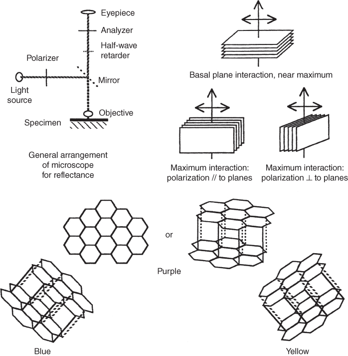
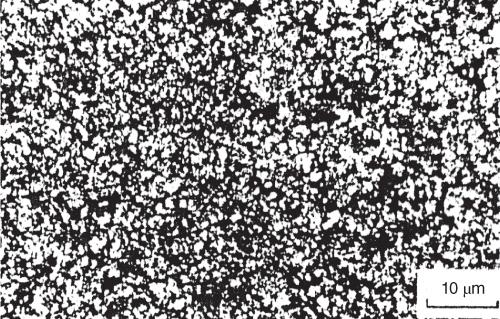
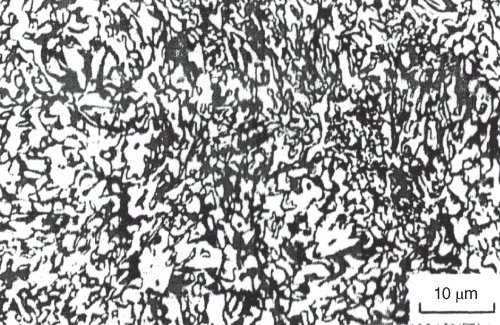
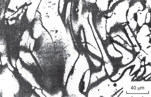
Nomenclature used to describe optical texture
OTI factor
Isotropic (Is and Ip)
No optical activity
0
Fine mosaics (F)
<0.8 µm in diameter
1
Medium mosaics (M)
>0.8 to <2.0 µm in diameter
3
Coarse mosaics (C)
>2.0 to <10.0 µm in diameter
7
Granular flow (GF)
>2 µm in length
7
>1 µm in width
Coarse flow (CF)
>10 µm in length
20
>2 µm in width
Lamellar (L)
>20 µm in length
30
>10 µm in width
17.4 Thermogravimetry
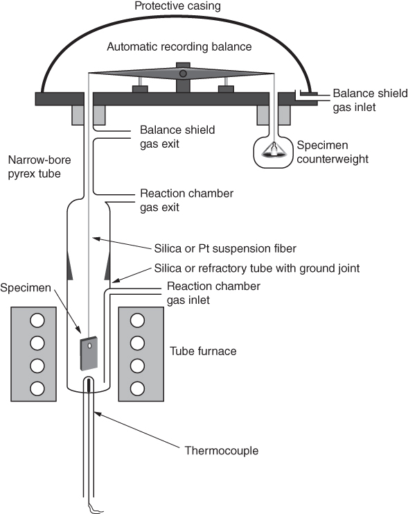
17.4.1 Buoyancy
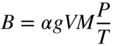
17.4.2 Convection Currents
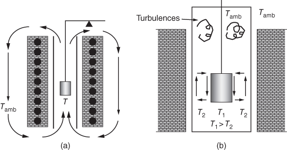
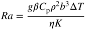

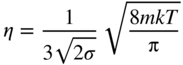
17.4.3 Thermomolecular Fluxes

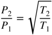
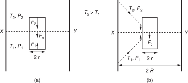
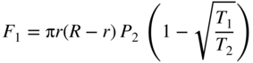
Knudsen number
Pressure domain (mbar; air, 298 K, R = 5 cm)
Type of gas flow
Observations
104–1
10−7–10−3
Thermomolecular
Knudsen forces
1–10−5
10−3–100
Intermediate
Knudsen forces
≤10−5
≥100
Convection
Fluctuations around an equilibrium position
Primary excitation
Detected emission
Methods of analysis: name and nomenclature
Photons, optical
Optical
Spectroscopy
Electrons
UPS: vacuum UV photoelectron spectroscopy
Outer shell
Photons
Electrons
XPS: X‐ray photoelectron spectroscopy
X‐rays
X‐rays
Inner shell; also called ESCA
ESCA: electron spectroscopy for chemical analysis
XFS: X‐ray fluorescence spectrometry
XRD: X‐ray diffraction
Electrons
X‐rays
EPMA: electron probe microanalysis
Electrons
SEM: scanning electron microscopy
TEM: transmission electron microscopy
STEM: scanning transmission electron microscopy
SAM: scanning AUGER microanalysis
AES: Auger electron spectroscopy
Ions
Optical
SCANIIR: surface composition by analysis of neutral and ion impact radiation
X‐rays
IIXA: ion‐induced X‐ray analysis
Ions (±)
ToFMS: time‐of‐flight mass spectrometry
SIMS: secondary ion mass spectrometry
IPM: ion probe microanalysis
ISS: ion scattering spectrometry
RBS: Rutherford backscattering spectrometry
Radiation
Optical
ES: emission spectroscopy
Ions (±)
SSMS: spark source mass spectrography
17.5 Spectroscopy
Characteristic
AES
XPS
ISS
SIMS
RBS
NRA
IXX
Sample alteration
High for alkali
halogen organic
insulators
Low
Low
Low
Very low
Very low
Very low
Elemental analysis
Good
Good
Good
Poor
Fair
Fair
Good
Sensitivity, variation, resolution
Good
Good
Fair
Good
Fair
Good
Good
Detection limits
0.1%
0.1%
0.1%
10−4% or higher
10−3% or higher
10−2% or higher
10−2% or higher
Chemical state
Yes
Yes
No
Yes
No
No
No
Quantification
With difficulty, required standards
With difficulty, required standards
With difficulty, required standards
With difficulty, required standards
Absolute, no standards
Absolute, no standards
Absolute, no standards
Lateral resolution
100 nm
2 mm
100 m
100 to 1 m
1 mm
1 mm
1 mm
Depth resolution
200 nm
To atomic layer
To atomic layer
To atomic layer
10 nm
10 nm
None
Depth analysis
Destructive, sputter
Destructive, sputter
Destructive, sputter
Destructive, sputter
Nondestructive
Nondestructive
Very difficult
Technique
Abbreviation
Information
Comments
Optical microscopy
OM
Surface topography and morphology
Inexpensive but modest resolving power and depth of field
Transmission electron microscopy
TEM
Surface topography and morphology
Very high resolution but requires replication; artifacts can be a serious problem
Scanning electron microscopy
SEM
Surface topography and morphology combined with X‐ray spectroscopy gives “bulk” elemental analysis
Resolving power > optical microscopy; preparation easier than TGEM and artifacts much less likely
X‐ray photoelectron spectrometry
XPS (ESCA)
Chemical composition, depth profiling
Especially useful for studying adhesion of polymers to metals
Secondary ion mass spectroscopy
SIMS
Elemental analysis in “monolayer range,” chemical composition, and depth profiling
Extremely high sensitivity for many elements
Auger electron spectroscopy
AES
Chemical composition, depth profiling, and lateral analysis
High spatial resolution that makes the technique especially suitable for composition–depth profiling
Contact angle measurement
—
Contamination by organic compounds
Inexpensive; rapid
Required sample analysis
Appropriate technique
Depth profiling lower Z elements and thin films; trace or minor analysis of light elements; quantitative analysis
NRA
Depth profiling of higher Z elements and thin films; trace analysis of heavy elements in light matrix; quantitative analysis
RBS
Trace, minor, and major element analysis in thicker samples; quantitative analysis
IIX
Minor and major elements at surface or interface of small samples
AES
Trace elements at surface or interface of medium to small size samples; analysis of insulators; sputter profiling of light elements
SIMS
Chemical state analysis; analyses of organics and insulators
XPS
Analysis of outer atom layer; analysis of insulators
ISS 
17.6 Diffraction Techniques
17.6.1 X‐Ray Diffraction
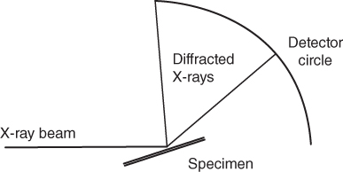
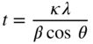
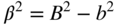
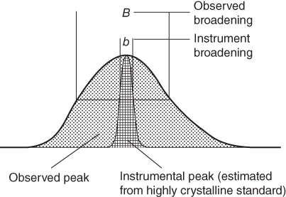
17.6.2 Low‐Energy Electron Diffraction
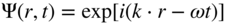
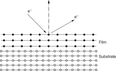
17.6.3 Reflection High‐Energy Electron Diffraction
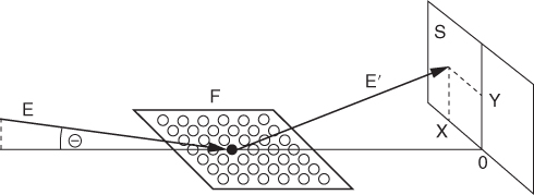
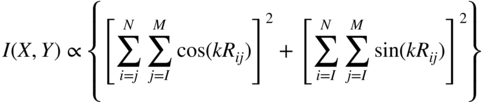
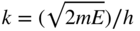
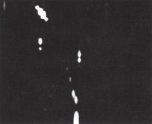
17.6.4 Neutron Scattering

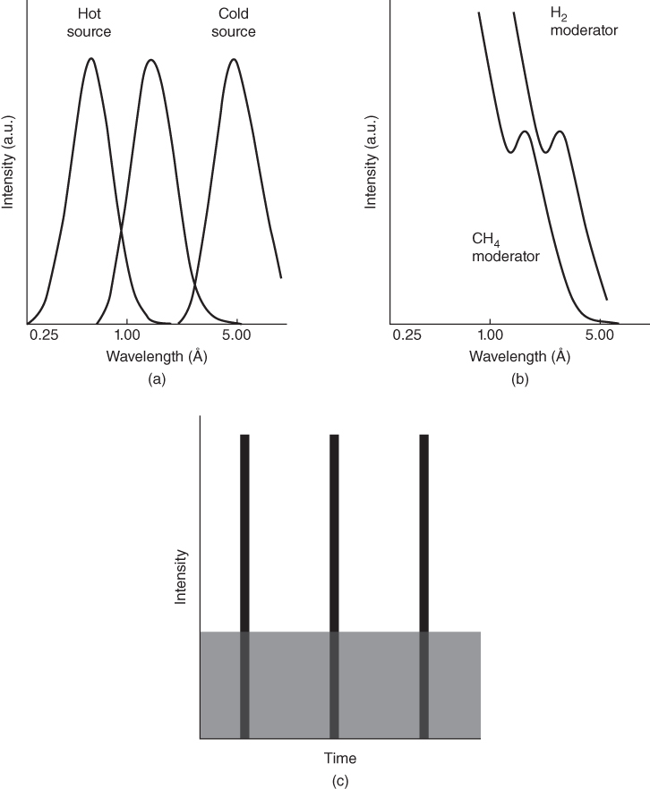
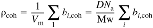
Nucleus
b/(10−12 cm)
1H
−0.3741
2H (D)
0.6671
12C
0.6646
16O
0.5803
19F
0.5650
23Na
0.3580
31P
0.5131
32S
0.2847
Cl
0.9577
Molecule
ρ/(1010 cm−2)
Water
H2O
−0.560
D2O
6.356
Heptane
C7H16
−0.548
C7D16
6.301
AOT
(C8H17COO)CH2CHSO3
0.542
(Na+)
(C8D17COO)CH2CHSO3
5.180a
(Na+)
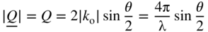

17.7 Electron Microscopy
17.7.1 Scanning Electron Microscopy
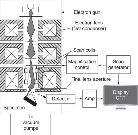
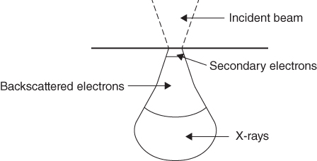
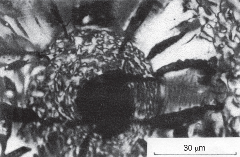
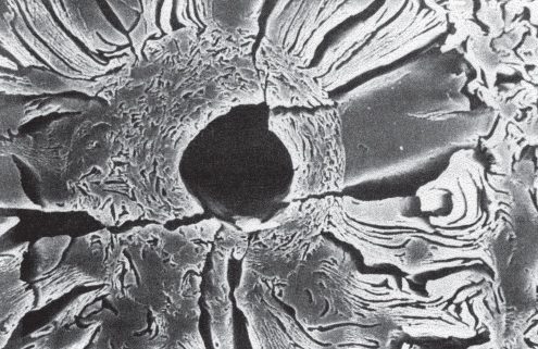
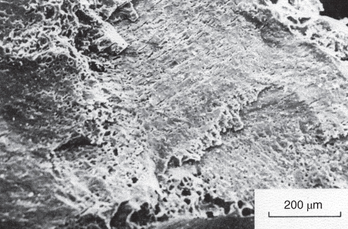
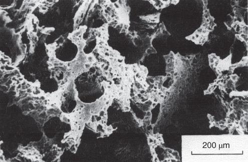
17.7.2 Transmission Electron Microscopy
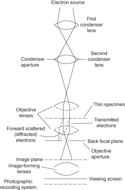
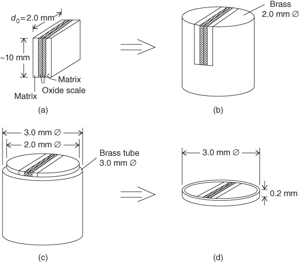
17.7.3 High‐Resolution Transmission Electron Microscopy
17.7.4 Low‐Energy Electron Microscopy
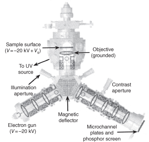
17.8 Electron Spectroscopy and Ion Scattering
17.8.1 Extended X‐Ray Absorption Fine Structure
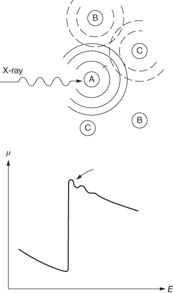
Transmission EXAFS
The standard measurement mode is transmission
Fluorescent EXAFS (or FLEXAFS)
Complementary to transmission mode, where X‐ray emission is detected particularly for dilute elements
XANES
Refers to the near‐edge structure, usually the first 100 eV above the edge that, through multiple scattering, is also sensitive to local symmetry
SOXAFS
Soft (energy) EXAFS, e.g. 800 eV to 8 keV, particularly for K edges of light elements
SEXAFS
Surface EXAFS, usually by photoelectron detection
REFLEXAFS
SEXAFS performed by using the fluorescent mode with glancing incident X‐rays totally externally reflected from the surface
QEXAFS
Quick EXAFS scans (∼1 min)
ED‐EXAFS
Energy‐dispersive EXAFS: a geometry for extremely rapid EXAFS scans, dispersing the transmitted beam and measuring by fast position‐sensitive detector
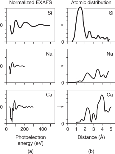
17.8.2 Photoemission
17.8.3 Auger and X‐Ray Photoelectron Spectroscopy
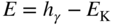
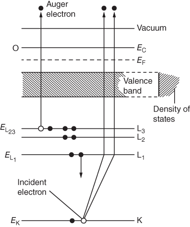
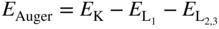
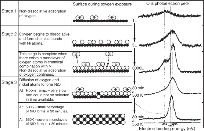
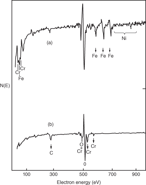
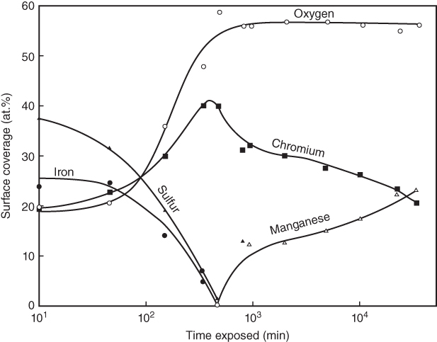
17.8.4 Rutherford Backscattering
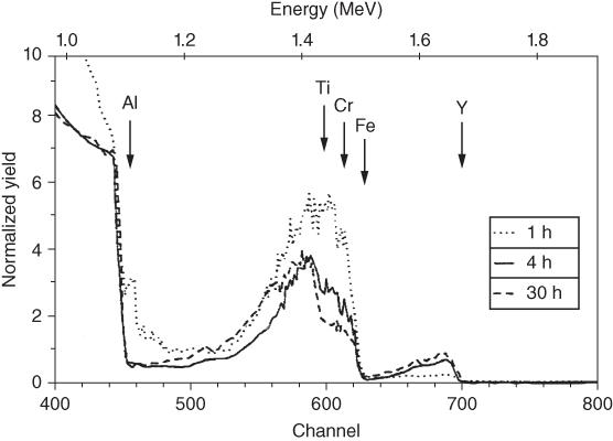
17.8.5 Secondary Ion Mass Spectrometry
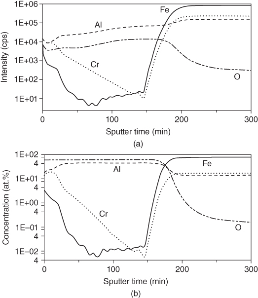
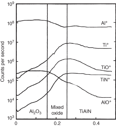
17.8.6 Ion Scattering Spectroscopy
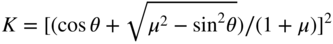

17.8.7 Low‐Energy Electron Loss Spectroscopy
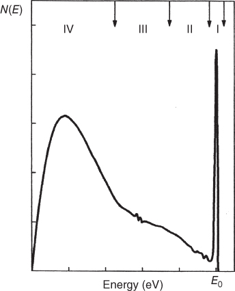
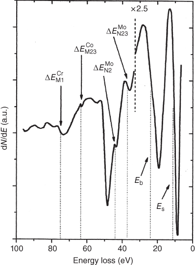

 is the elastic scattering factor of electrons. Λβ is the effective free path of electrons in a sample with respect to inelastic collisions, which is determined by the equation
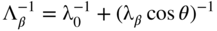
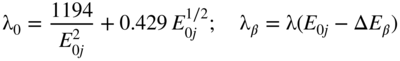
17.9 Surface Microscopy
17.9.1 Scanning Tunneling Microscopy
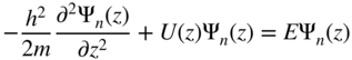
17.9.2 Atomic Force Microscopy
STM
AFM
Instrumentation
Tip, scanner, controller
Cantilever, scanner, optics controller
Conducting samples
Yes
Yes
Nonconducting samples
No
Yes
Resolution in vacuum
<0.1 Å
∼Å
In dry air
<1 Å
∼nm
In liquid
∼nm
∼10 nm
Operation in liquid
Tip coating
No coating needed
Modes of operation
Constant height
Constant height
Constant current
Constant force
Contact mode
Tapping mode
Applications
Imaging
Imaging
Tunneling spectroscopy
Force mapping
Manipulation of atoms/molecules
Nanolithography
17.9.3 Surface Force Apparatus
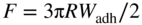

17.9.4 Lateral Force Microscopy


17.10 Optical Spectroscopy
17.10.1 Luminescence
17.10.2 Light Scattering


 . Consequently, light scattering concerns the positions of atoms relative to their neighbors rather than to the individual movement of individual particles and therefore resembles coherent rather than incoherent neutron scattering.
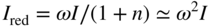
17.10.3 Ellipsometry


17.10.4 Optical Spectroscopy in the Infrared, Visible, and Ultraviolet
17.10.4.1 Electromagnetic Radiation Light
 , is
, is
 are frequently used to characterize IR radiation with the units given in cm−1. The interaction between matter and electromagnetic radiation is easiest to understand if we assume that radiation consists of a beam of energetic particles called photons. When a photon is absorbed by a sample, it is “destroyed,” and its energy (in joules), acquired by the sample, being related to its frequency, wavelength, and wavenumber by the following equalities:
Type of energy transfer
Region of electromagnetic spectrum
Spectroscopic technique
Absorption
γ‐ray
Mossbauer spectroscopy
X‐ray
X‐ray absorption spectroscopy
UV/Vis
UV/Vis spectroscopy
Atomic absorption spectroscopy
IR
Infrared spectroscopy
Raman spectroscopy
Microwave
Microwave spectroscopy
Radio wave
Electron spin resonance spectroscopy
Nuclear magnetic resonance spectroscopy
Emission (thermal excitation)
UV/Vis
Atomic emission spectroscopy
Photoluminescence
X‐ray
X‐ray fluorescence
UV/Vis
Fluorescence spectroscopy
Phosphorescence spectroscopy
Atomic fluorescence spectroscopy
Chemiluminescence
UV/Vis
Chemiluminescence spectroscopy

 , is
, is


Transition
Wavelength range (nm)
Examples
σ → σ*
<200
CC, CH
n → σ*
160–260
H2O, CH3OH, CH3Cl
π → π*
200–500
C=C, C=O, C=N, CC
n → π*
250–600
C=O, C=N, N=N, N=O

17.10.5 Fourier Transform Infrared Spectroscopy
17.10.5.1 Attenuated Total Reflectance
17.10.6 Nonlinear Optical Spectroscopy

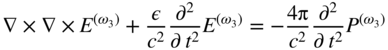


 is
is
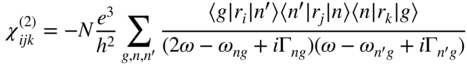
 carries eight terms describing the different time ordering of the photons. The multiplication of three matrix elements in each term presents the coupling of the photons with matter in three separate steps. The summation indicates that the process must go over all possible excited states. One of the possible matrix processes is shown in Figure 17.49.


 represents its value in the lab frame and can be transformed to the crystal frame by a rotation operator. Using Eqs. 17.46 and 17.47, we can rewrite the expression as


17.11 Nondestructive Inspection Techniques
17.11.1 Fluorescent Penetrant Inspection
17.11.2 Eddy Current

17.11.3 Frequency Scanning Eddy Current Technique
17.11.4 Ultrasonic Inspection
17.11.5 Infrared Imaging
17.11.6 Pulse‐Echo Thermal Wave Infrared Imaging
17.11.7 Phase of Thermal Emission Spectroscopy
17.11.8 Acoustic Emission
17.11.9 Mid‐Infrared Reflectance


17.11.10 Photoluminescence Piezospectroscopy

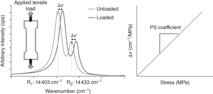
17.11.11 Interferometric Techniques
17.11.12 Thermal Wave Interferometry

17.11.13 Holography
17.11.14 Shearography
17.11.15 Electron Backscatter Diffraction

17.11.16 Glow Discharge Optical Emission Spectrometry
17.12 Traditional Electrochemical Methods
17.12.1 Potentiometry
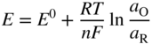


 , and Al2Cl6. By fitting the experimental cell voltage with models involving different species, information about the existence of these species and the equilibrium constants for equilibrium reactions in which they participate have been derived. The chemistry and electrochemistry of chalcogens, such as tellurium, selenium, and sulfur, in chloroaluminate melts have been investigated in a similar way as well as the formation of chloride complexes for certain transition metal ions. The existence of different low oxidation states and the constants of the relevant equilibrium reactions have been derived from the experimentally measured cell voltages (Mamantov 1978).
17.12.2 Chronoamperometry

 is the bulk concentration of the oxidized species initially present in the solution (mol cm−3), and DO is the diffusion coefficient of the oxidized species (cm2 s−1).


17.12.3 Chronopotentiometry
 in the LiCl–KCl eutectic at 423 °C at a gold electrode is shown in Figure 17.59.
17.12.4 Chronocoulometry


17.12.5 Cyclic Voltammetry

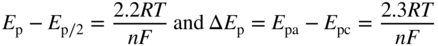
17.12.6 Linear Sweep Voltammetry

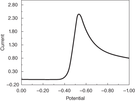
17.12.7 Normal and Differential Pulse Voltammetry


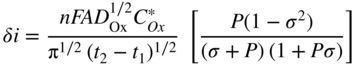

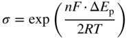

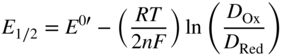
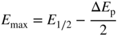

17.12.8 Square Wave Voltammetry


17.12.9 Rotating Disk and Rotating Ring‐Disk Voltammetry

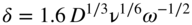
 is given by Eq. 17.80 written here for a reduction process:
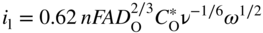

 and
and  are the cathodic and anodic limiting currents, respectively. E1/2 is related to the formal potential of the redox couple, E0′, by the expression
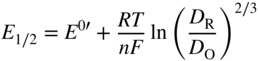

17.12.10 Charge and Capacitance Measurements

 , then the coverage, θ, is given by

 may not correspond to complete coverage of the surface. To relate θ as measured in Eq. 17.85 with the true surface area, at least on platinum, it is common to measure the charge passed in oxidation of the hydride region of the cyclic voltammogram. This charge, denoted QH, takes the value 210 µC cm−2 for smooth polycrystalline platinum and is largely independent of the sweep rate. Furthermore, if a partial electrode film is already present, the hydride layer will only form on the unoccupied part of the surface, and if the hydride oxidation charge is now
  , then

17.13 Nontraditional Electrochemical Methods
17.13.1 AC Impedance Plots


17.13.2 Electrochemical Noise

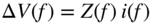

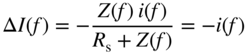


17.13.3 Solid‐State Voltammetry


 . The standard potential of the Cu2O/Cu electrode with respect to the reversible oxygen electrode (ROE) at 1 atm O2 (or unitary fugacity of oxygen),
  , could be calculated from thermodynamic data. A correction of the potential scale of the measurements on the samples can then be made according to Eq. 17.102:


 is related to
  by the Nernst equation

 is equal to 1.

17.14 Combined Electrochemical Methods
17.14.1 Scanning Electrochemical Microscopy


17.14.2 Infrared Spectroelectrochemistry

17.14.3 Electrochemical Surface Forces Apparatus

17.14.4 Electrochemical Electron Spin Resonance

 . The energy of this dipole in an external magnetic induction, B, is


17.14.5 Electrochemical Mass Spectroscopy


17.14.6 Electrochemical STM

17.14.7 Electrochemical AFM
17.14.8 Electroreflectance Spectroscopy
 (i.e. the dielectric constant as a function of frequency), the imaginary part of which signifies absorption. In the early days of electroreflectance spectroscopy, the spectra were often interpreted in terms of the dielectric functions of the participating media. However, dielectric functions are macroscopic concepts, ill suited to the description of surfaces, interfaces, or thin layers. It is therefore preferable to interpret the data in terms of the electronic transitions involved wherever possible.
17.14.9 Second Harmonic Generation
17.14.10 Scanning Tunneling Microscope


17.14.11 Electrochemical Surface‐Enhanced Raman Spectroscopy
Electrochemistry
EC‐Raman spectroscopy
ECSTM
Sensitivity
Submonolayer
Submonolayera
Submonolayer
Energy resolution
10−2 V
10−4 eV (∼1 cm−1)b
STS is not availablec
Spatial resolution
0.1–1 µmd
1 µm
1 Å
Time resolution (s)
10−7–10−6
10−8e–10−3f
0.04g


17.14.12 Electrochemical Quartz Crystal Microbalance
17.14.13 Electrochemical Strain Microscopy


References
Further Reading
Testing and Evaluation
17.1
17.2
17.3
17.4
17.5
17.6
17.7
17.8
17.9
17.10
17.11
17.12
17.13
17.14
17.15
17.16
17.17
17.18
17.19
17.20
17.21
17.22
17.23
17.24
17.25
17.26
17.27
17.28
17.29
17.30
17.31
17.32
17.33
17.34
17.35
17.36
17.37
17.38
17.39
17.40
17.41
17.42
17.43
17.44
17.45
17.46
17.47
17.48
17.49
17.50
17.51
17.52
17.53
17.54
17.55
17.56
17.57
17.58
17.59
17.60
17.61
17.62
17.63
17.64
17.65
17.66
17.67
17.68
17.69
17.70
17.71
17.72
17.73
17.74
17.75
17.76
17.77
17.78
17.79
17.80
17.81
17.82
17.83
17.84
17.85
17.86
17.87
17.88
17.89
17.90
17.91
17.92
17.93
17.94
17.95
17.96
17.97
17.98
17.99
17.100
17.101
17.102
17.103
17.104
17.105
17.106
17.107
17.108
17.109
17.110
17.111
17.112
17.113
17.114